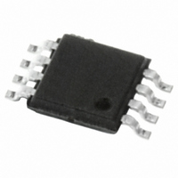
M95040-WDW6TP STMicroelectronics, M95040-WDW6TP Datasheet - Page 9

M95040-WDW6TP
Manufacturer Part Number
M95040-WDW6TP
Description
IC EEPROM 4KBIT 10MHZ 8TSSOP
Manufacturer
STMicroelectronics
Datasheet
1.M95010-WMN6TP.pdf
(43 pages)
Specifications of M95040-WDW6TP
Format - Memory
EEPROMs - Serial
Memory Type
EEPROM
Memory Size
4K (512 x 8)
Speed
10MHz
Interface
SPI, 3-Wire Serial
Voltage - Supply
2.5 V ~ 5.5 V
Operating Temperature
-40°C ~ 85°C
Package / Case
8-TSSOP
Organization
512 x 8
Interface Type
SPI
Maximum Clock Frequency
5 MHz
Supply Voltage (max)
5.5 V
Supply Voltage (min)
2.5 V
Maximum Operating Current
2 mA
Maximum Operating Temperature
+ 85 C
Mounting Style
SMD/SMT
Minimum Operating Temperature
- 40 C
Operating Supply Voltage
3.3 V, 5 V
Lead Free Status / RoHS Status
Lead free / RoHS Compliant
Other names
497-8679-2
M95040-WDW6TP
M95040-WDW6TP
Available stocks
Company
Part Number
Manufacturer
Quantity
Price
Part Number:
M95040-WDW6TP
Manufacturer:
ST
Quantity:
20 000
M95040, M95020, M95010
2.6
2.7
2.8
2.9
2.9.1
2.9.2
Write Protect (W)
This input signal is used to control whether the memory is write protected. When Write
Protect (W) is held low, writes to the memory are disabled, but other operations remain
enabled. Write Protect (W) must either be driven high or low, but must not be left floating.
V
V
Supply voltage (V
Supply voltage (V
Operating supply voltage V
Prior to selecting the memory and issuing instructions to it, a valid and stable V
within the specified [V
Table
instruction and, for a Write instruction, until the completion of the internal write cycle (t
order to secure a stable DC supply voltage, it is recommended to decouple the V
a suitable capacitor (usually of the order of 10 nF to 100 nF) close to the V
pins.
Device reset
In order to prevent inadvertent write operations during power-up, a power-on-reset (POR)
circuit is included. At power-up, the device does not respond to any instruction until V
reaches the internal reset threshold voltage (this threshold is defined in
Table 10
When V
●
●
●
When V
Power mode. The device must not be accessed until V
voltage within the specified [V
Table
SS
SS
is the reference for the V
in Standby Power mode
deselected (note that, to be executed, an instruction must be preceded by a falling
edge on Chip Select (S))
Status register value:
–
–
–
10). This voltage must remain stable and valid until the end of the transmission of the
10.
ground
CC
CC
as V
the Write Enable Latch (WEL) is reset to 0
Write In Progress (WIP) is reset to 0
The SRWD, BP1 and BP0 bits remain unchanged (non-volatile bits)
passes over the POR threshold, the device is reset and is in the following state:
passes over the POR threshold, the device is reset and enters the Standby
RES
).
CC
(min), V
CC
CC
CC
CC
)
)
Doc ID 6512 Rev 8
CC
(min), V
supply voltage.
CC
(max)] range must be applied (see
CC
(max)] range defined in
CC
reaches a valid and stable V
Table
Table
Table
Signal description
8,
CC
Table 9
8,
/V
8,
Table 9
CC
SS
Table 9
CC
package
voltage
line with
and
CC
W
CC
and
). In
and
9/43


