CY62148DV30LL-55SXI Cypress Semiconductor Corp, CY62148DV30LL-55SXI Datasheet - Page 3
CY62148DV30LL-55SXI
Manufacturer Part Number
CY62148DV30LL-55SXI
Description
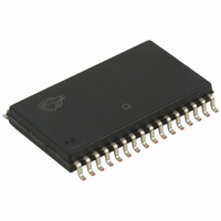
IC SRAM 4MBIT 55NS 32SOIC
Manufacturer
Cypress Semiconductor Corp
Type
Asynchronousr
Specifications of CY62148DV30LL-55SXI
Memory Size
4M (512K x 8)
Package / Case
32-SOIC (11.30mm Width)
Format - Memory
RAM
Memory Type
SRAM
Speed
55ns
Interface
Parallel
Voltage - Supply
2.2 V ~ 3.6 V
Operating Temperature
-40°C ~ 85°C
Access Time
55 ns
Supply Voltage (max)
3.6 V
Supply Voltage (min)
2.2 V
Maximum Operating Current
10 mA
Maximum Operating Temperature
+ 85 C
Minimum Operating Temperature
- 40 C
Mounting Style
SMD/SMT
Number Of Ports
1
Operating Supply Voltage
2.5 V, 3.3 V
Lead Free Status / RoHS Status
Lead free / RoHS Compliant
Lead Free Status / RoHS Status
Lead free / RoHS Compliant, Lead free / RoHS Compliant
Other names
428-2074-5
CY62148DV30LL-55SXI
CY62148DV30LL-55SXI


Document #: 38-05341 Rev. *D
Maximum Ratings
(Exceeding maximum ratings may impair the useful life of the
device. For user guidelines, not tested.)
Storage Temperature .................................. –65°C to +150°C
Ambient Temperature with
Power Applied............................................... 55°C to +125°C
Supply Voltage to Ground
Potential ......................................... –0.3V to V
DC Voltage Applied to Outputs
in High-Z State
DC Input Voltage
Electrical Characteristics
Notes:
V
V
V
V
I
I
I
I
I
Parameter
IX
OZ
CC
SB1
SB2
5. V
6. V
7. Full device AC operation assumes a 100 µs ramp time from 0 to V
OH
OL
IH
IL
IL(min)
IH(max)
= –2.0V for pulse durations less than 20 ns.
= V
CC
Output HIGH
Voltage
Output LOW
Voltage
Input HIGH
Voltage
Input LOW
Voltage
Input Leakage
Current
Output Leakage
Current
V
Supply Current
Automatic CE
Power-down
Current —
CMOS Inputs
Automatic CE
Power-down
Current —
CMOS Inputs
+0.75V for pulse durations less than 20 ns.
[5, 6]
CC
Description
[5, 6]
Operating
......................... –0.3V to V
..................... –0.3V to V
I
I
I
I
V
V
V
V
GND < V
GND < V
f = f
f = 1 MHz
CE > V
V
f = f
f = 0 (OE, and WE), V
CE > V
V
f = 0, V
OH
OH
OL
OL
CC
CC
CC
CC
IN
IN
Over the Operating Range
>V
= 0.1 mA
= 2.1 mA
= –0.1 mA V
= –1.0 mA V
max
max
> V
= 2.7V to 3.6V
= 2.7V to 3.6V
= 2.2V to 2.7V
= 2.2V to 2.7V
CC
CC
CC
CC
CC
(Address and Data Only),
= 1/t
I
O
–0.2V, V
< V
−0.2V,
– 0.2V,
= 3.60V
< V
– 0.2V or V
RC
CC
CC
CC(max)
CC(max)
CC(max)
Test Conditions
, Output Disabled
V
V
V
I
CMOS levels
OUT
IN
CC
CC
CC
CC
CC
<0.2V)
= 2.20V
= 2.70V
= 2.20V
= 2.70V
= V
= 0 mA
CC
IN
+ 0.3V
+ 0.3V
+ 0.3V
CC(min)
< 0.2V,
=3.60V
CC(max)
and 200 µs wait time after V
Output Current into Outputs (LOW)............................. 20 mA
Static Discharge Voltage.......................................... > 2001V
(per MIL-STD-883, Method 3015)
Latch-up Current..................................................... > 200 mA
Operating Range
CY62148DV30L
CY62148DV30LL
CY62148DV30LL Automotive-A –40°C to +85°C
Auto-A LL
Auto-A LL
Auto-A LL
Auto-A LL
Ind’l
Ind’l
Ind’l
Ind’l
Ind’l
Ind’l
Ind’l
Ind’l
Product
L
LL
L
LL
L
LL
L
LL
–0.3
–0.3
Min Typ
2.0
2.4
1.8
2.2
–1
–1
CC
stabilization.
55 ns
1.5
1.5
Industrial
8
8
2
2
2
2
Range
[4]
V
V
Max
0.3V
0.3V
0.4
0.4
0.6
0.8
CC
CC
+1
+1
15
10
12
12
3
3
8
8
+
+
–40°C to +85°C 2.2V to
–0.3
–0.3
Min Typ
2.0
2.4
1.8
2.2
–1
–1
Temperature
CY62148DV30
Ambient
70 ns
1.5
1.5
8
8
2
2
2
2
[4]
Page 3 of 10
V
V
Max
0.3V
0.3V
0.4
0.4
0.6
0.8
CC
CC
+1
+1
10
10
3
3
8
8
8
8
+
+
V
3.6V
CC
Unit
mA
mA
mA
mA
mA
mA
µA
µA
µA
µA
V
V
V
V
V
V
V
V
[7]
Related parts for CY62148DV30LL-55SXI
Image
Part Number
Description
Manufacturer
Datasheet
Request
R

Part Number:
Description:
Manufacturer:
Cypress Semiconductor Corp
Datasheet:
Part Number:
Description:
Manufacturer:
Cypress Semiconductor Corp
Datasheet:
Part Number:
Description:
Manufacturer:
Cypress Semiconductor Corp
Datasheet:
Part Number:
Description:
Manufacturer:
Cypress Semiconductor Corp
Datasheet:
Part Number:
Description:
Manufacturer:
Cypress Semiconductor Corp
Datasheet: