CY62148DV30LL-55SXI Cypress Semiconductor Corp, CY62148DV30LL-55SXI Datasheet - Page 4
CY62148DV30LL-55SXI
Manufacturer Part Number
CY62148DV30LL-55SXI
Description
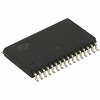
IC SRAM 4MBIT 55NS 32SOIC
Manufacturer
Cypress Semiconductor Corp
Type
Asynchronousr
Specifications of CY62148DV30LL-55SXI
Memory Size
4M (512K x 8)
Package / Case
32-SOIC (11.30mm Width)
Format - Memory
RAM
Memory Type
SRAM
Speed
55ns
Interface
Parallel
Voltage - Supply
2.2 V ~ 3.6 V
Operating Temperature
-40°C ~ 85°C
Access Time
55 ns
Supply Voltage (max)
3.6 V
Supply Voltage (min)
2.2 V
Maximum Operating Current
10 mA
Maximum Operating Temperature
+ 85 C
Minimum Operating Temperature
- 40 C
Mounting Style
SMD/SMT
Number Of Ports
1
Operating Supply Voltage
2.5 V, 3.3 V
Lead Free Status / RoHS Status
Lead free / RoHS Compliant
Lead Free Status / RoHS Status
Lead free / RoHS Compliant, Lead free / RoHS Compliant
Other names
428-2074-5
CY62148DV30LL-55SXI
CY62148DV30LL-55SXI


Document #: 38-05341 Rev. *D
AC Test Loads and Waveforms
Capacitance
Thermal Resistance
Data Retention Characteristics
Data Retention Waveform
Notes:
V
I
t
t
C
C
Parameter
Parameter
CCDR
CDR
R
8. Tested initially and after any design or process changes that may affect these parameters.
9. Full Device AC operation requires linear V
Parameter
DR
IN
OUT
[9]
Θ
Θ
[8]
JA
JC
V
CE
Parameters
CC
OUTPUT
Input Capacitance
Output Capacitance
Thermal Resistance
(Junction to Ambient)
Thermal Resistance
(Junction to Case)
R
V
V
Data Retention Current
Chip Deselect to Data Retention Time
Operation Recovery Time
R1
R2
TH
TH
CC
V
INCLUDING
(for all packages)
CC
for Data Retention
JIG AND
SCOPE
Description
Description
50 pF
Description
R1
[8]
CC
2.5V (2.2V – 2.7V)
R2
ramp from V
T
Still Air, soldered on a 3 x 4.5
inch, four-layer printed circuit
board
(Over the Operating Range)
A
t
CDR
= 25°C, f = 1 MHz, V
1.5V
16667
15385
8000
1.20
Equivalent to:
Test Conditions
DR
to V
V
V
CC(min)
CC
IN
> V
OUTPUT
= 1.5V, CE > V
Rise Time: 1 V/ns
V
CC
DATA RETENTION MODE
> 100 µs or stable at V
CC
GND
Test Conditions
− 0.2V or V
CC
THÉ VENIN EQUIVALENT
= V
V
DR
CC(typ)
10%
3.0V (2.7V – 3.6V)
Conditions
CC
> 1.5 V
IN
− 0.2V,
< 0.2V
VFBGA
R
1554
CC(min)
1103
8.86
TH
1.75
ALL INPUT PULSES
645
72
90%
Ind’l/Auto-A LL
> 100 µs.
V
Ind’l
TH
TSOP II
75.13
8.95
1.5V
L
90%
t
R
10%
Fall time: 1 V/ns
Min Typ
1.5
t
RC
0
CY62148DV30
SOIC
Max
55
22
10
10
Unit
Ω
Ω
Ω
V
[4]
Page 4 of 10
Max
9
6
°C/W
°C/W
Unit
Unit
pF
pF
Unit
µA
µA
ns
ns
V
Related parts for CY62148DV30LL-55SXI
Image
Part Number
Description
Manufacturer
Datasheet
Request
R

Part Number:
Description:
Manufacturer:
Cypress Semiconductor Corp
Datasheet:
Part Number:
Description:
Manufacturer:
Cypress Semiconductor Corp
Datasheet:
Part Number:
Description:
Manufacturer:
Cypress Semiconductor Corp
Datasheet:
Part Number:
Description:
Manufacturer:
Cypress Semiconductor Corp
Datasheet:
Part Number:
Description:
Manufacturer:
Cypress Semiconductor Corp
Datasheet: