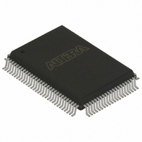
EPC4QI100N Altera, EPC4QI100N Datasheet - Page 46

EPC4QI100N
Manufacturer Part Number
EPC4QI100N
Description
IC CONFIG DEVICE 4MBIT 100-PQFP
Manufacturer
Altera
Series
EPCr
Datasheet
1.EPC4QI100N.pdf
(116 pages)
Specifications of EPC4QI100N
Programmable Type
In System Programmable
Memory Size
4Mb
Voltage - Supply
3 V ~ 3.6 V
Operating Temperature
-40°C ~ 85°C
Package / Case
100-MQFP, 100-PQFP
Lead Free Status / RoHS Status
Lead free / RoHS Compliant
Other names
544-2190
Available stocks
Company
Part Number
Manufacturer
Quantity
Price
Company:
Part Number:
EPC4QI100N
Manufacturer:
ALTERA
Quantity:
300
Part Number:
EPC4QI100N
Manufacturer:
ALTERA/阿尔特拉
Quantity:
20 000
2–10
Configuration Handbook (Complete Two-Volume Set)
f
Logical Divisions
In all enhanced configuration devices, configuration option bits are stored ranging
from word address 0x008000 to 0x00801F (byte address 0x010000 to 0x01003F).
These bits are used to enable various controller features such as configuration mode
selection, compression mode selection, and clock divider selection. In all enhanced
configuration devices, configuration data is stored starting from word address
location 0x008020 or byte address 0x010040. The ending address of configuration
space is not fixed and depends on the number and density of PLDs configured using
the enhanced configuration device as well as the number of pages. All remaining
address locations above the configuration space are available for processor
application code. The boot space spans addresses 0x000000 to 0x007FFF. Both boot
and application code spaces are intended for use by an external processor or PLD.
Figure 2–10
Figure 2–10. EPC16 Flash Memory Map
Physical Divisions
Conversely, physical divisions are flash data blocks that can be individually written to
and erased. For instance, the Sharp flash-based EPC16 device contains 16-Mbit Sharp
flash memory that is divided into 2 boot blocks, 6 parameter blocks, and 31 main data
blocks. These physical divisions vary from one flash memory or vendor to another
and must be considered if the external flash interface is used to erase or write flash
memory. These divisions are not significant if the interface is used as a read-only
interface after initial programming.
For detailed information about enhanced configuration device flash memories, refer
to the following documents:
■
■
■
For Micron flash-based EPC4, refer to the Micron Flash Memory MT28F400B3 Data
Sheet at www.micron.com.
For Sharp flash-based EPC16, refer to the Sharp LHF16J06 Data Sheet Flash Memory
Used in EPC16 Devices at www.sharpsma.com.
For the Intel Advanced Boot Block Flash Memory (B3) 28F008/800B3, 28F016/160B3,
28F320B3, 28F640B3 Datasheet, visit www.intel.com.
shows the flash memory map inside an EPC16 device.
Addresses
Word
Specifications
Processor
0x00801F
0x008020
0x000000
Boot/Parameter Blocks
Configuration Pages
Flash Memory Map
Application Code
Unused Memory
Option Bits
Chapter 2: Altera Enhanced Configuration Devices
0xFFFFFF
© December 2009 Altera Corporation
Configuration
Space
External Flash Memory Interface


