EPC4QI100N Altera, EPC4QI100N Datasheet - Page 86
EPC4QI100N
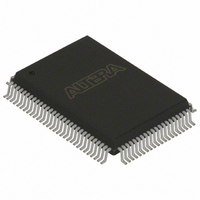
Manufacturer Part Number
EPC4QI100N
Description
IC CONFIG DEVICE 4MBIT 100-PQFP
Manufacturer
Altera
Series
EPCr
Datasheet
1.EPC4QI100N.pdf
(116 pages)
Specifications of EPC4QI100N
Programmable Type
In System Programmable
Memory Size
4Mb
Voltage - Supply
3 V ~ 3.6 V
Operating Temperature
-40°C ~ 85°C
Package / Case
100-MQFP, 100-PQFP
Lead Free Status / RoHS Status
Lead free / RoHS Compliant
Other names
544-2190
Available stocks
Company
Part Number
Manufacturer
Quantity
Price
Company:

Part Number:
EPC4QI100N
Manufacturer:
ALTERA
Quantity:
300
Part Number:
EPC4QI100N
Manufacturer:
ALTERA/阿尔特拉
Quantity:
20 000


3–34
Table 3–23. Serial Configuration Device Pin Description (Part 2 of 2)
Package
Configuration Handbook (Complete Two-Volume Set)
nCS
DCLK
V
GND
Name
CC
Pin
1
6
3, 7, 8
4
Pin Number
Package
f
in 8-Pin
SOIC
As shown in
16-pin device. In order to take advantage of vertical migration from EPSCS1 to
EPCS128, Altera recommends a layout for serial configuration devices.
Figure 3–23. Layout Recommendation for Vertical Migration from EPCS1 to EPCS128
EPCS1 and EPCS4 available in 8-pin small outline integrated circuit (SOIC) package.
EPCS16 available in 8-pin and 16-pin small outline integrated circuit (SOIC) packages.
EPCS64 and EPCS128 available in 16-pin small outline integrated circuit (SOIC)
package.
For more information about Altera device packaging including mechanical drawing
and specifications for this package, refer to the
Sheet.
7
16
1, 2, 9
10
Pin Number
in 16-Pin
Package
SOIC
Chapter 3: Serial Configuration Devices (EPCS1, EPCS4, EPCS16, EPCS64, and EPCS128) Data Sheet
Figure 3–21
Input
Input
Power
Ground
Pin Type
and
The active low chip select input signal toggles at the beginning and
end of a valid instruction. When this signal is high, the device is
deselected and the DATA pin is tri-stated. When this signal is low, it
enables the device and puts the device in an active mode. After power
up, the serial configuration device requires a falling edge on the nCS
signal before beginning any operation.
DCLK is provided by the FPGA. This signal provides the timing of the
serial interface. The data presented on ASDI is latched to the serial
configuration device on the rising edge of DCLK. Data on the DATA
pin changes after the falling edge of DCLK and is latched into the
FPGA on the next falling edge.
Power pins connect to 3.3 V.
Ground pin.
Figure
3–22, the serial configuration device is an 8-pin or
Pin 1 ID
Altera Device Package Information Data
Description
© December 2009
Altera Corporation
Package
Related parts for EPC4QI100N
Image
Part Number
Description
Manufacturer
Datasheet
Request
R

Part Number:
Description:
Sram-based LUT Devices
Manufacturer:
Altera Corporation
Datasheet:

Part Number:
Description:
(EPC4 / EPC8 / EPC16) Enhanced Configuration Devices
Manufacturer:
Altera
Datasheet:

Part Number:
Description:
CYCLONE II STARTER KIT EP2C20N
Manufacturer:
Altera
Datasheet:
Part Number:
Description:
CPLD, EP610 Family, ECMOS Process, 300 Gates, 16 Macro Cells, 16 Reg., 16 User I/Os, 5V Supply, 35 Speed Grade, 24DIP
Manufacturer:
Altera Corporation
Datasheet:
Part Number:
Description:
CPLD, EP610 Family, ECMOS Process, 300 Gates, 16 Macro Cells, 16 Reg., 16 User I/Os, 5V Supply, 15 Speed Grade, 24DIP
Manufacturer:
Altera Corporation
Datasheet:
Part Number:
Description:
Manufacturer:
Altera Corporation
Datasheet:
Part Number:
Description:
CPLD, EP610 Family, ECMOS Process, 300 Gates, 16 Macro Cells, 16 Reg., 16 User I/Os, 5V Supply, 30 Speed Grade, 24DIP
Manufacturer:
Altera Corporation
Datasheet:
Part Number:
Description:
High-performance, low-power erasable programmable logic devices with 8 macrocells, 10ns
Manufacturer:
Altera Corporation
Datasheet:
Part Number:
Description:
High-performance, low-power erasable programmable logic devices with 8 macrocells, 7ns
Manufacturer:
Altera Corporation
Datasheet:
Part Number:
Description:
Classic EPLD
Manufacturer:
Altera Corporation
Datasheet:
Part Number:
Description:
High-performance, low-power erasable programmable logic devices with 8 macrocells, 10ns
Manufacturer:
Altera Corporation
Datasheet:
Part Number:
Description:
Manufacturer:
Altera Corporation
Datasheet:
Part Number:
Description:
Manufacturer:
Altera Corporation
Datasheet: