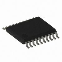
AT18F040-30XU Atmel, AT18F040-30XU Datasheet

AT18F040-30XU
Specifications of AT18F040-30XU
Related parts for AT18F040-30XU
AT18F040-30XU Summary of contents
Page 1
... The AT18F Series Configurators can be programmed with Atmel or industry-standard, third-party, stand-alone programmers such as BP, Data I/O, Hi-Lo, etc. AT18F002 AT18F040 AT18F080 2 Mbit 4 Mbit Yes 3.3V 1.8-3.3V 1.8-3.3V 33 MHz 20-lead TSSOP Yes FPGA Configuration Flash Memory AT18F010 AT18F002 AT18F040 AT18F080 Preliminary 7 Mbit 3672A–CNFG–1/08 ...
Page 2
Pin Configuration 3. Block Diagram Power-on Reset Internal Oscillator Flash Memory AT18F010/002/040/080 [Preliminary] 2 20-lead TSSOP DATA CLK 3 18 TDI 4 17 TMS 5 16 TCK RESET/OE 8 ...
Page 3
... CLK pin of an AT18F series device as a configuration loading clock. Multiple FPGAs that are setup in Master Serial and Slave Serial modes can also be used to control the configuration pro- cess to obtain data from a single configurator or cascaded configurators. Please contact Atmel at configurator@atmel.com for detailed descriptions. ...
Page 4
... Spartan-3 XC3S400 XC2S150E Spartan-IIE XC2S200E XC2S300E Spartan-II XC2S200 Atmel Xilinx Virtex-II Pro XC2VP4 XC2V500 Virtex-II XC2V1000 XCV400E Virtex-E XCV405E XCV600E XCV400 AT18F040-30XU Virtex XCV600 XC3S500E Spartan-3E XC3S1200E Spartan-3L XC3S1000L Spartan-3 XC3S1000 XC2S400E Spartan-IIE XC2S600E Virtex-5 LX XC5VLX30 XC4VLX15 Virtex-4 LX XC4VLX25 XC4VFX12 Virtex-4 FX ...
Page 5
... To allow ISP programming support by the Automated Test Equipment (ATE) vendors, Serial Vector Format (SVF) files can be created by the Atmel JCPS Software. Conversion to other ATE tester format beside SVF is also possible AT18Fxx devices can also be programmed using standard third-party programmers such as BP, DataI/O, Hi-Lo, etc ...
Page 6
Pin Description Table 6-1. Name DATA CLK RESET/ CEO TMS TCK TDI TDO VCCINT NC VCCO GND VCCJ 6.1 DATA (D0) Open-collector bi-directional data pin. This pin has an internal 20 KΩ pull-up resistor. 6.2 CLK Clock ...
Page 7
CEO Chip Enable Output for configuration download. This output goes Low when the internal address counter of the device has reached its maximum value which signals that all configuration data is being clocked out of the device ...
Page 8
... Configuration Memory to FPGA Device Interface Connection Diagrams Figure 8-1. General Connection Diagram for Loading FPGA from Configurator and JTAG Signals Notes: 1. Signals within parenthesis will be applied to Atmel AT40AK FPGA. 2. For details of the circuit connection, please contact factory. AT18F010/002/040/080 [Preliminary] 8 3672A–CNFG–1/08 ...
Page 9
Absolute Maximum Ratings* Operating Temperature................................. -55° +125° C Storage Temperature .................................... -65 ° +150° C Voltage on Any Pin with Respect to Ground ..............................-0. Supply Voltage (V ) .........................................-0.5V to +3.6V CC Maximum ...
Page 10
DC Characteristics Symbol Description I Internal Voltage Supply Current, Active Mode CCINT I I/O Drive Supply Current, Active Mode CCIO I JTAG Supply Current, Active Mode CCJ I Internal Voltage Supply Current, Standby Mode CCINTS I Output Drive Supply ...
Page 11
AC Characteristics Figure 12-1. AT18Fxx as Configuration Slave with CLK Input Pin as Clock Source CE T SCE RESET/OE CLK DATA Table 12-1. AC Characteristics over Operating Conditions Symbol Description T CF ...
Page 12
Figure 12-2. AC Characteristics when Cascading RESET/OE CE CLK DATA LAST BIT CEO Table 12-2. AC Characteristics When Cascading Symbol Description T CLK to Output Float Delay CDF T CLK to CEO Delay OCK CEO Delay OCE ...
Page 13
... Wide, Plastic Think-Shrink Small Outline (TSSOP) 3672A–CNFG–1/08 AT18F010/002/040/080 [Preliminary] Ordering Code AT18F010-30XU 20A2 - 20 TSSOP AT18F002-30XU 20A2 - 20 TSSOP AT18F040-30XU 20A2 - 20 TSSOP AT18F080-30XU 20A2 - 20 TSSOP Package Type Package Operation Range Industrial (-40° 85° C) Industrial (-40° 85° C) Industrial (-40° ...
Page 14
Packaging Information 14.1 20A2 – TSSOP b Marked Pin1 Indentifier Top View e 0.10 mm TYP Top View Side View e1 Bottom View Notes: 1. This drawing is for general ...
Page 15
Revision History Revision Level – Release Date A – January 2008 3672A–CNFG–1/08 AT18F010/002/040/080 [Preliminary] History Initial release. 15 ...
Page 16
... Disclaimer: The information in this document is provided in connection with Atmel products. No license, express or implied, by estoppel or otherwise, to any intellectual property right is granted by this document or in connection with the sale of Atmel products. EXCEPT AS SET FORTH IN ATMEL’S TERMS AND CONDI- TIONS OF SALE LOCATED ON ATMEL’S WEB SITE, ATMEL ASSUMES NO LIABILITY WHATSOEVER AND DISCLAIMS ANY EXPRESS, IMPLIED OR STATUTORY WARRANTY RELATING TO ITS PRODUCTS INCLUDING, BUT NOT LIMITED TO, THE IMPLIED WARRANTY OF MERCHANTABILITY, FITNESS FOR A PARTICULAR PURPOSE, OR NON-INFRINGEMENT ...


