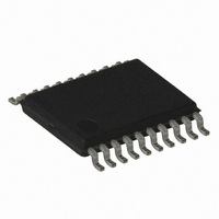
AT18F040-30XU Atmel, AT18F040-30XU Datasheet - Page 6

AT18F040-30XU
Manufacturer Part Number
AT18F040-30XU
Description
IC FLASH CONFIG 4MBIT 20-TSSOP
Manufacturer
Atmel
Datasheet
1.AT18F010-30XU.pdf
(16 pages)
Specifications of AT18F040-30XU
Programmable Type
FLASH
Memory Size
4Mb
Voltage - Supply
3 V ~ 3.6 V
Operating Temperature
-40°C ~ 85°C
Package / Case
20-TSSOP (0.173", 4.40mm Width)
Lead Free Status / RoHS Status
Lead free / RoHS Compliant
6. Pin Description
6.1
6.2
6.3
6.4
6.5
6
DATA (D0)
CLK
RESET/OE
CE
CF
AT18F010/002/040/080 [Preliminary]
Table 6-1.
Open-collector bi-directional data pin. This pin has an internal 20 KΩ pull-up resistor.
Clock input. Used to increment the internal address and bit counter for reading and program-
ming. This pin has an internal 20 KΩ pull-up resistor.
Output Enable (active High) and RESET (active Low). A Low level on RESET/OE resets both
the address and bit counters. A High level (with CE Low) enables the data output driver. This pin
has an internal 20 KΩ pull-up resistor.
Chip Enable input (active Low). A Low level (with OE High) allows CLK to increment the address
counter and enables the data output driver. A High level on CE disables both the address and bit
counters and forces the device into a low-power standby mode. This pin has an internal 20 KΩ
pull-up resistor.
Configuration Pulse (open-drain output). Allows JTAG CONFIG instruction to initiate FPGA con-
figuration without powering down the FPGA. This is an open-drain output that is pulsed Low by
the JTAG CONFIG command.
Name
DATA
CLK
RESET/OE
CE
CF
CEO
TMS
TCK
TDI
TDO
VCCINT
NC
VCCO
GND
VCCJ
Pin Descriptions
Power Supply
Power Supply
Ground
Type
I/O
O
O
-
I
I
I
I
I
I
I
I
2, 9, 12, 14, 15, 16
20-lead TSSOP
10
13
17
18
19
11
20
5
1
3
8
7
6
4
3672A–CNFG–1/08


