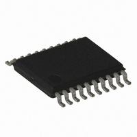
AT18F040-30XU Atmel, AT18F040-30XU Datasheet - Page 7

AT18F040-30XU
Manufacturer Part Number
AT18F040-30XU
Description
IC FLASH CONFIG 4MBIT 20-TSSOP
Manufacturer
Atmel
Datasheet
1.AT18F010-30XU.pdf
(16 pages)
Specifications of AT18F040-30XU
Programmable Type
FLASH
Memory Size
4Mb
Voltage - Supply
3 V ~ 3.6 V
Operating Temperature
-40°C ~ 85°C
Package / Case
20-TSSOP (0.173", 4.40mm Width)
Lead Free Status / RoHS Status
Lead free / RoHS Compliant
6.6
6.7
6.8
6.9
6.10
6.11
6.12
6.13
6.14
6.15
7. Standby Mode
3672A–CNFG–1/08
CEO
TMS
TCK
TDI
TDO
VCCINT
NC
VCCO
VCCJ
GND
Chip Enable Output for configuration download. This output goes Low when the internal address
counter of the device has reached its maximum value which signals that all configuration data is
being clocked out of the device. In a daisy chain of AT18F Series devices, the CEO pin of one
device must be connected to the CE input of the next device in the chain. It will stay Low as long
as CE is Low and OE is High. It will then follow CE until OE goes Low; thereafter, CEO will stay
High until the entire memory device is read again.
JTAG Mode Control Input. The state of TMS with the rising edge of TCK determines the state
transitions of the Test Access Port (TAP) controller. TMS has an internal 50 KΩ weak pull-up to
V
JTAG Clock Input. This pin is the JTAG clock input to the TAP controller of the device.
JTAG Serial Data Input. This pin is the serial input to all JTAG instructions and data registers. An
internal 50 KΩ weak pull-up to V
JTAG Serial Data Output. This pin is the serial output to all JTAG instruction and data registers.
An internal 50 KΩ weak pull-up to V
+3.3V supply voltage for internal logic.
No Connect Pin. This pin is not connected to any internal logic of the device and can be left
floating.
Supply voltage for I/O drivers (1.8V, 3.3V, or 3.3V).
Supply voltage for JTAG I/O drivers (1.8V, 3.3V, or 3.3V).
Power supply ground.
The AT18F Series Configurators enter a low-power standby mode whenever the JTAG mode is
inactive and CE is asserted High. In this mode, the AT18F Configurator consumes less than 1
mA of current at 3.3V. The output remains in a high-impedance state regardless of the state of
the OE input.
CCJ
to provide a logic 1 to the device.
AT18F010/002/040/080 [Preliminary]
CCJ
CCJ
provides a logic 1 to the device.
provides a logic 1 to the device if the pin is not driven.
7


