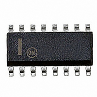
MC33363BDWR2G ON Semiconductor, MC33363BDWR2G Datasheet - Page 2

MC33363BDWR2G
Manufacturer Part Number
MC33363BDWR2G
Description
IC OFFLINE SWIT PWM HV 16SOIC
Manufacturer
ON Semiconductor
Type
High Voltage Switching Regulatorr
Datasheet
1.MC33363BDWG.pdf
(11 pages)
Specifications of MC33363BDWR2G
Output Isolation
Isolated
Frequency Range
59 ~ 315kHz
Voltage - Input
9.5 ~ 40 V
Voltage - Output
700V
Operating Temperature
-25°C ~ 150°C
Package / Case
16-SOIC (0.300", 7.50mm Width) 13 leads
Output Voltage Range
5.5 V to 7.5 V
Input Voltage Range
40 V
Mounting Style
SMD/SMT
Lead Free Status / RoHS Status
Lead free / RoHS Compliant
Other names
MC33363BDWR2GOS
MC33363BDWR2GOS
MC33363BDWR2GOSTR
MC33363BDWR2GOS
MC33363BDWR2GOSTR
Available stocks
Company
Part Number
Manufacturer
Quantity
Price
Company:
Part Number:
MC33363BDWR2G
Manufacturer:
ON Semiconductor
Quantity:
3 200
Part Number:
MC33363BDWR2G
Manufacturer:
ON/安森美
Quantity:
20 000
Stresses exceeding Maximum Ratings may damage the device. Maximum Ratings are stress ratings only. Functional operation above the
Recommended Operating Conditions is not implied. Extended exposure to stresses above the Recommended Operating Conditions may affect
device reliability.
1. This device series contains ESD protection and exceeds the following tests:
2. Maximum power dissipation limits must be observed.
3. Tested junction temperature range for the MC33363B: T
MAXIMUM RATINGS
ELECTRICAL CHARACTERISTICS
for min/max values T
REGULATOR (Pin 8)
OSCILLATOR (Pin 7)
ERROR AMPLIFIER (Pins 9, 10)
Power Switch (Pin 16)
Startup Input Voltage (Pin 1, Note 2)
Power Supply Voltage (Pin 3)
Input Voltage Range
Thermal Characteristics
Operating Junction Temperature
Storage Temperature
Output Voltage (I
Line Regulation (V
Load Regulation (I
Total Output Variation over Line, Load, and Temperature
Frequency
Frequency Change with Voltage (V
Voltage Feedback Input Threshold
Line Regulation (V
Input Bias Current (V
Open Loop Voltage Gain (T
Gain Bandwidth Product (f = 100 kHz, T
Output Voltage Swing
Drain Voltage
Drain Current
Voltage Feedback Input (Pin 10)
Compensation (Pin 9)
Overvoltage Protection Input (Pin 11)
R
C
P Suffix, Dual--In--Line Case 648E
DW Suffix, Surface Mount Case 751G
C
C
High State (I
Low State (I
Thermal Resistance, Junction--to--Air
Thermal Resistance, Junction--to--Case
Thermal Resistance, Junction--to--Air
Thermal Resistance, Junction--to--Case
T
T
T
T
T
T
T
T
Human Body Model 2000 V per MIL--STD--883, Method 3015.
Machine Model Method 200 V.
J
J
J
J
(Pin 6)
(Pin 7)
= 390 pF
= 2.0 nF
= 25C (V
= T
= 25C (V
= T
low
low
to T
to T
Sink
Source
CC
CC
high
high
O
= 100 mA, V
O
= 20 V)
= 20 V)
CC
CC
= 0 mA, T
J
(V
(V
= 100 mA, V
= 0 mA to 10 mA)
FB
is the operating junction temperature range that applies (Note 3), unless otherwise noted.)
= 20 V to 40 V)
= 20 V to 40 V, T
CC
CC
(Note 1)
= 2.6 V, T
= 20 V to 40 V)
= 20 V to 40 V)
J
Characteristic
J
= 25C)
FB
= 25C)
FB
> 3.0 V)
J
CC
< 2.0 V)
= 0 -- 125C)
= 20 V to 40 V)
Rating
J
J
= 25C)
= 25C)
(V
CC
= 20 V, R
http://onsemi.com
low
T
= --25C
= 10 k, C
2
T
T
high
= 390 pF, C
Δf
Symbol
Reg
Reg
Reg
= +125C
OSC
GBW
A
f
V
V
V
V
V
OSC
I
VOL
OH
reg
reg
IB
OL
FB
load
line
line
/ΔV
Pin 8
Symbol
R
R
R
R
V
V
T
I
V
V
T
DS
2.52
0.85
θJA
θJC
θJA
θJC
Min
stg
260
255
DS
CC
= 1.0 mF, for typical values T
5.5
5.3
4.0
IR
60
59
70
in
J
--
--
--
--
--
--
67.5
Typ
285
6.5
0.1
2.6
0.6
1.0
5.3
0.2
30
44
20
82
--
--
--
--25 to +150
--55 to +150
--1.0 to V
Value
700
500
1.0
40
80
15
95
15
reg
Max
2.68
1.15
0.35
500
200
310
315
500
7.5
8.0
2.0
5.0
75
76
94
--
J
= 25C,
C/W
MHz
Unit
Unit
kHz
kHz
mV
mV
mV
C
C
nA
dB
V
A
V
V
V
V
V
V
V


