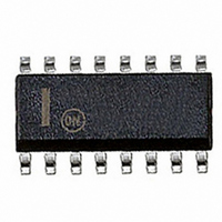
MC33363BDWR2G ON Semiconductor, MC33363BDWR2G Datasheet - Page 9

MC33363BDWR2G
Manufacturer Part Number
MC33363BDWR2G
Description
IC OFFLINE SWIT PWM HV 16SOIC
Manufacturer
ON Semiconductor
Type
High Voltage Switching Regulatorr
Datasheet
1.MC33363BDWG.pdf
(11 pages)
Specifications of MC33363BDWR2G
Output Isolation
Isolated
Frequency Range
59 ~ 315kHz
Voltage - Input
9.5 ~ 40 V
Voltage - Output
700V
Operating Temperature
-25°C ~ 150°C
Package / Case
16-SOIC (0.300", 7.50mm Width) 13 leads
Output Voltage Range
5.5 V to 7.5 V
Input Voltage Range
40 V
Mounting Style
SMD/SMT
Lead Free Status / RoHS Status
Lead free / RoHS Compliant
Other names
MC33363BDWR2GOS
MC33363BDWR2GOS
MC33363BDWR2GOSTR
MC33363BDWR2GOS
MC33363BDWR2GOSTR
Available stocks
Company
Part Number
Manufacturer
Quantity
Price
Company:
Part Number:
MC33363BDWR2G
Manufacturer:
ON Semiconductor
Quantity:
3 200
Part Number:
MC33363BDWR2G
Manufacturer:
ON/安森美
Quantity:
20 000
Introduction
integration by providing all the active high voltage power,
control,
implementation of a flyback or forward converter on a single
monolithic chip. This device is designed for direct operation
from a rectified 240 Vac line source and requires a minimum
number of external components to implement a complete
converter. A description of each of the functional blocks is
given below, and the representative block and timing
diagrams are shown in Figures 19, 18 and 20.
Oscillator and Current Mirror
selected for the timing components R
programs the oscillator charge/discharge current via the
Current Mirror 4 I output, Figure 4. Capacitor C
and discharged by an equal magnitude internal current
source and sink. This generates a symmetrical 50 percent
duty cycle waveform at Pin 7, with a peak and valley
threshold of 2.6 V and 0.6 V respectively. During the
discharge of C
pulse that holds the inverting input of the AND gate Driver
high. This causes the Power Switch gate drive to be held in
a low state, thus producing a well controlled amount of
output deadtime. The amount of deadtime is relatively
constant with respect to the oscillator frequency when
operating below 1.0 MHz. The maximum Power Switch
duty cycle at Pin 16 can be modified from the internal 50%
limit by providing an additional charge or discharge current
path to C
cycle, a discharge current resistor R
Pin 7 to ground. To decrease the maximum duty cycle, a
charge current resistor R
Regulator Output. Figure 5 shows an obtainable range of
maximum output duty cycle versus the ratio of either R
R
D
The MC33363B represents a new higher level of
The oscillator frequency is controlled by the values
with respect to R
Figure 21. Maximum Duty Cycle Modification
R C
R D
T
, Figure 21. In order to increase the maximum duty
Regulator Output
and
T
C
1.0
, the oscillator generates an internal blanking
R
T
T
protection
T
8
6
7
.
I
C
is connected from Pin 7 to the
Comparator
Current
Mirror
circuitry
Oscillator
PWM
4 I
T
D
2.25 I
and C
is connected from
Current
Limit
Reference
required
T
OPERATING DESCRIPTION
Blanking
Pulse
. Resistor R
T
is charged
http://onsemi.com
C
for
or
T
9
the oscillator frequency are given below. The frequency
formula is a first order approximation and is accurate for C
values greater than 500 pF. For smaller values of C
to Figure 2. Note that resistor R
Limit Comparator threshold.
PWM Comparator and Latch
the oscillator ramp voltage applied to the non- -inverting input,
while the error amplifier output is applied into the inverting
input. The Oscillator applies a set pulse to the PWM Latch
while C
Power Switch conduction is initiated. When C
voltage that exceeds the error amplifier output, the PWM
Latch is reset, thus terminating Power Switch conduction for
the duration of the oscillator ramp- -up period. This
PWM Comparator/Latch combination prevents multiple
output pulses during a given oscillator clock cycle. The
timing diagram shown in Figure 18 illustrates the Power
Switch duty cycle behavior versus the Compensation voltage.
Current Limit Comparator and Power Switch
means of protecting the output switch transistor from
overstress. Each on- -cycle is treated as a separate situation.
Current limiting is implemented by monitoring the output
switch current buildup during conduction, and upon sensing
an overcurrent condition, immediately turning off the switch
for the duration of the oscillator ramp- -up period.
a virtually lossless method of monitoring the drain current. It
consists of a total of 1462 cells, of which 36 are connected to
a 8.1 Ω ground- -referenced sense resistor. The Current Sense
Comparator detects if the voltage across the sense resistor
exceeds the reference level that is present at the inverting
input. If exceeded, the comparator quickly resets the PWM
Latch, thus protecting the Power Switch. The current limit
reference level is generated by the 2.25 I output of the Current
Mirror. This current causes a reference voltage to appear
across the 405 Ω resistor. This voltage level, as well as the
Oscillator charge/discharge current are both set by resistor R
Therefore when selecting the values for R
be chosen first to set the Power Switch peak drain current,
while C
frequency. A graph of the Power Switch peak drain current
versus R
below.
The formula for the charge/discharge current along with
The pulse width modulator consists of a comparator with
The MC33363B uses cycle- -by- -cycle current limiting as a
The Power Switch is constructed as a SENSEFET allowing
I
T
chg∕dscg
T
T
is discharging, and upon reaching the valley voltage,
is shown in Figure 3 with the related formula
is chosen second to set the desired Oscillator
I
pk
=
= 8.8
5.4
R T
1000
R T
T
also programs the Current
--
1.077
f ≈
T
I
chg∕dscg
and C
4C
T
charges to a
T
T
, R
T
T
, refer
must
T
T
.


