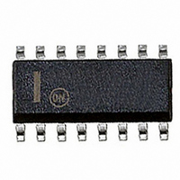
MC33363BDWR2G ON Semiconductor, MC33363BDWR2G Datasheet - Page 5

MC33363BDWR2G
Manufacturer Part Number
MC33363BDWR2G
Description
IC OFFLINE SWIT PWM HV 16SOIC
Manufacturer
ON Semiconductor
Type
High Voltage Switching Regulatorr
Datasheet
1.MC33363BDWG.pdf
(11 pages)
Specifications of MC33363BDWR2G
Output Isolation
Isolated
Frequency Range
59 ~ 315kHz
Voltage - Input
9.5 ~ 40 V
Voltage - Output
700V
Operating Temperature
-25°C ~ 150°C
Package / Case
16-SOIC (0.300", 7.50mm Width) 13 leads
Output Voltage Range
5.5 V to 7.5 V
Input Voltage Range
40 V
Mounting Style
SMD/SMT
Lead Free Status / RoHS Status
Lead free / RoHS Compliant
Other names
MC33363BDWR2GOS
MC33363BDWR2GOS
MC33363BDWR2GOSTR
MC33363BDWR2GOS
MC33363BDWR2GOSTR
Available stocks
Company
Part Number
Manufacturer
Quantity
Price
Company:
Part Number:
MC33363BDWR2G
Manufacturer:
ON Semiconductor
Quantity:
3 200
Part Number:
MC33363BDWR2G
Manufacturer:
ON/安森美
Quantity:
20 000
1.80 V
1.75 V
1.70 V
--20
--40
--60
--80
8.0
32
24
16
--50
0
0
0
Figure 8. Error Amplifier Small Signal
I
D
--25
Figure 12. Power Switch Drain- -Source
= 200 mA
Figure 10. Regulator Output Voltage
On- -Resistance versus Temperature
I
Change versus Source Current
4.0
reg
, REGULATOR SOURCE CURRENT (mA)
T
0
Transient Response
A
, AMBIENT TEMPERATURE (C)
Pulse tested at 5.0 ms with < 1.0% duty cycle
so that T
25
8.0
1.0 ms/DIV
J
is as close to T
50
12
75
A
as possible.
V
R
C
T
100
V
A
C
T
A
CC
T
Pin 8
A
V
CC
L
= 25C
= 10 k
= --1.0
= 10 pF
= 25C
= 20 V
16
= 20 V
= 1.0 mF
125
http://onsemi.com
150
20
5
3.00 V
1.75 V
0.50 V
160
120
80
40
0
6
5
4
3
2
1
0
1.0
0
C
Drain- -Source Capacitance versus Voltage
OSS
Figure 9. Error Amplifier Large Signal
measured at 1.0 MHz with 50 mVpp.
2.0
Figure 11. Peak Startup Current
versus Power Supply Voltage
V
V
Figure 13. Power Switch
DS
CC
Transient Response
, DRAIN--SOURCE VOLTAGE (V)
, POWER SUPPLY VOLTAGE (V)
4.0
10
1.0 ms/DIV
6.0
100
8.0
V
A
C
T
A
V
T
CC
V
L
V
T
A
Pin 1
= 25C
A
= --1.0
= 10 pF
CC
= 25C
= 20 V
= 25C
10
= 20 V
= 50 V
1000
12


