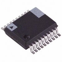
ADE7753ARSZ Analog Devices Inc, ADE7753ARSZ Datasheet - Page 48

ADE7753ARSZ
Manufacturer Part Number
ADE7753ARSZ
Description
IC ENERGY METERING 1PHASE 20SSOP
Manufacturer
Analog Devices Inc
Datasheet
1.ADE7753ARSZ.pdf
(60 pages)
Specifications of ADE7753ARSZ
Input Impedance
390 KOhm
Measurement Error
0.1%
Voltage - I/o High
2.4V
Voltage - I/o Low
0.8V
Current - Supply
3mA
Voltage - Supply
4.75 V ~ 5.25 V
Operating Temperature
-40°C ~ 85°C
Mounting Type
Surface Mount
Package / Case
20-SSOP (0.200", 5.30mm Width)
Meter Type
Single Phase
Ic Function
Single-Phase Multifunction Metering IC
Supply Voltage Range
4.75V To 5.25V
Operating Temperature Range
-40°C To +85°C
Digital Ic Case Style
SSOP
No. Of Pins
20
Lead Free Status / RoHS Status
Lead free / RoHS Compliant
For Use With
EVAL-ADE7753ZEB - BOARD EVALUATION AD7753
Lead Free Status / RoHS Status
Lead free / RoHS Compliant, Lead free / RoHS Compliant
Available stocks
Company
Part Number
Manufacturer
Quantity
Price
Part Number:
ADE7753ARSZ
Manufacturer:
ADI/亚德诺
Quantity:
20 000
Part Number:
ADE7753ARSZRL
Manufacturer:
ADI/亚德诺
Quantity:
20 000
ADE7753
ADE7753 SERIAL INTERFACE
All ADE7753 functionality is accessible via several on-chip
registers—see Figure 89. The contents of t
updated or read using the on-chip serial interface. After power-
on o
ADE7753 is placed in communications mode. In communica-
tions
regis
determines whether the next data transfer operation
a write and also which register is accessed. Therefore all data
transfer operations with the ADE7753, whether a read or a
writ
The communications reg
determines whether the n
a write. The six LSBs contain the address of the register to be
accessed—see the Communications Register section for a more
detailed description.
Figure 90 and Figure 91 show the data transfer sequences for a
read and write operation, respectively. On completion of a data
transfer (read or write), the ADE7753 once again enters
communications mode. A data transfer is complete when the
LSB of the ADE7753 register being addressed (for a write or a
read) is transferred to or from the AD
Figure 89. Addressing ADE7753 Registers via the Communications Register
e, must begin with
r toggling th
ter. The data writte
mode, t
DOUT
DIN
he AD
e RESET
E7753 exp
a write to the communications r
n to the communications register
ister is an 8-bit wide register. The MSB
REGISTER 1
REGISTER 2
REGISTER 3
REGISTER n–1
REGISTER n
ext data transfer operation is a read or
pin low or a falling edge on CS , t
COMMUNICATIONS
REGISTER
ects a write to its communications
E7753.
OUT
OUT
OUT
OUT
OUT
IN
IN
IN
IN
IN
hese registers can be
REGISTER
ADDRESS
DECODE
02875-0-078
is a read or
egister.
he
Rev. A | Page 48 of 60
DOUT
SCLK
The serial interface of the ADE7753 is made up of four signals:
SCLK, DIN, DOUT, and
is applied at the SCLK logic input. This logic input has a
Schmitt-trigger input structure that allows slow rising (and
falling) clock edges to be used. All data transfer operations
synchronized to the serial clock. Data is shifted into the
ADE7753 at the DIN logic in
Data is shifted out of the ADE7
on a rising edge of SCLK. The
input. This input is used when multiple devices share the serial
bus. A falling edge on CS also resets the serial interface and
places the ADE7753 into communications mode. The CS inpu
should be driven low for the entire data transfer operation.
Bringing
transfer and places the serial bus in a high impedance state. The
CS logic input can be tied low if the ADE7753 is the only device
on the serial bus. However, with CS tied low, all initiated data
transfer operations must be fully completed, i.e., the LSB of each
register must be transferred because there is no other way
bringing the ADE7753 back into communications mo
without resetting the entire device by using RESET .
SCLK
DIN
DIN
CS
CS
COMMUNICATIONS REGISTER WRITE
COMMUNICATIONS REGISTER WRITE
Figure 90. Reading
Figure 91. Writing Data to the ADE7753 via the Serial Interface
CS high during a data transfer operation aborts the
1
0
0
0
ADDRESS
ADDRESS
Data from the ADE7753 via
CS . The serial clock for a data transfer
put on the falling edge of SCLK.
CS
753 at the DOUT logic output
logic input is the chip-select
MULTIBYTE
MULTIBYTE READ DA
the Serial Inter
READ DATA
TA
de
face
02875-0-079
02875-0-08
of
are
t
0


