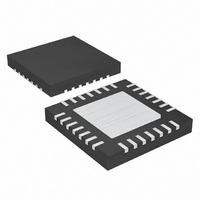
DS1864T+ Maxim Integrated Products, DS1864T+ Datasheet - Page 17

DS1864T+
Manufacturer Part Number
DS1864T+
Description
IC LASER CTRLR 1CHAN 5.5V 28TQFN
Manufacturer
Maxim Integrated Products
Type
Laser Diode Controller (Fiber Optic)r
Datasheet
1.DS1864TTR.pdf
(72 pages)
Specifications of DS1864T+
Number Of Channels
1
Voltage - Supply
2.97 V ~ 5.5 V
Current - Supply
3mA
Operating Temperature
-40°C ~ 95°C
Package / Case
28-WFQFN Exposed Pad
Mounting Type
Surface Mount
Lead Free Status / RoHS Status
Lead free / RoHS Compliant
current temperature. The DAC value referenced in the
LUT is then loaded into address 82h of Table 04h
(Table 01h in DS1859 configuration) for DAC0 and into
address 83h of Table 04h (Table 01h in DS1859 config-
uration) for DAC1.
During normal operation, the DAC setting is automati-
cally modified once per conversion cycle based on the
ADC results. However, if the TEN bit (bit 1, address
80h, Table 04h (Table 01h in DS1859 configuration)) is
set to 0, the DACs are placed in a manual mode and
temperature indexing is disabled. Once in manual
mode, the user programs the current-sink DACs by
writing the desired positions to addresses 82h and 83h
in Table 04h (Table 01h in DS1859 configuration) to
control DAC0 and DAC1, respectively.
The rate select pin (RSEL) along with the SELC rate
select bit (Lower Memory Register, byte 6Eh, bit 3)
determine the state of the RSELOUT pin, which is
intended to be used to control receiver multirate perfor-
mance. The RSEL pin state is OR’ed with the state of the
SELC bit to determine the RSELOUT pin state. Bit SELS
(Lower Memory Register, byte 6Eh, bit 4) indicates the
state of the RSEL pin. See Figure 13 for more details.
The DS1864 incorporates five basic monitor channels,
which include temperature, supply voltage (V
three external channels (MON1, MON2, and MON3).
These analog signals are sampled and converted into
digital measurements and compared to threshold limits
to determine alarm and warning signals and fault states.
These five signals can be calibrated externally, using
reserved registers for calibration values, or internally,
using built-in gain, offset, and right-shifting functions.
Table 1. LUT Addresses For
Corresponding Temperature Values
ADDRESS (hex)
C6
C7
80
81
82
⎯
Monitoring Features
TEMPERATURE (°C)
CORRESPONDING
≥ +102°C
≤ -40°C
+100°C
DAC Manual Mode
-38°C
-36°C
____________________________________________________________________
⎯
RSEL Operation
CC
), and
SFP Laser Controller and
In optical transceiver applications, the external monitor
channels are typically used for Bias Current (IBI)
through pins MON1P and MON1N, Transmitted Power
(TXP) through a MON2 pin, and Received Power (RIN)
through pins MON3P and MON3N. While MON2 is a
single-ended monitor, MON1 and 3 have the option of
being used as differential or single-ended monitors. To
use these channels single-ended, connect the ‘N’ side
to ground. A 13-bit ADC samples and digitizes the five
analog signals and the results are stored in registers
60h through 69h in the Lower Memory. The representa-
tive digital values are 13-bits wide (left justified), and
are stored in successive register pairs. The tempera-
ture value is stored in a 2’s complement format, while
V
signed format. The digital values are updated every
t
ings are generated after a digital comparison with high
and low set limits. A maskable interrupt, MINT, asserted
through TX-Fault, can be enabled based on any combi-
nation of alarms and warnings.
Alarm and warning flags are generated by comparing
the digitally converted values of the measured tempera-
ture, supply voltage, and three MON inputs with user-
programmed upper and lower limits. These limits are
stored in EEPROM locations 00h through 27h in the
Lower Memory. The two types of flags, alarm and warn-
ing, are also stored in the Lower Memory. Addresses
70h and 71h contain the alarm flags, while addresses
74h and 75h contain the warning flags. The Alarms and
Warnings section under Fault Management describe
how to program the alarm and warning thresholds, and
how to use them to generate interrupts.
Calibration is provided internally or externally. External
calibration makes use of a range of registers, reserved
for this purpose according to SFF-8472 standard. This
range is 38h to 5F in the Lower Memory Registers. The
calibration constants are loaded in the registers during
system test. In external calibration mode, a host
processor retrieves the constants and computes the
calibrated data.
The DS1864 features internal calibration for the five
analog channels. Internal calibration makes use of two
registers for four of the five monitored analog channels:
V
Power (TXP)) and MON3 (Received Power (RIN)). One
register is for offset calibration, the other for gain cali-
bration. Both registers are loaded during system test.
Only the offset scaling register is used for temperature.
FRAME
CC
CC
, MON1 (Bias Current (IBI)), MON2 (Transmitted
and the three analog inputs are stored in an un-
. From these measurements, alarms and warn-
Diagnostic IC
Alarm and Warning Flags
Calibration Overview
Digital Diagnostics
17


