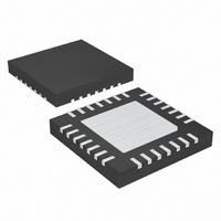
DS1864T+ Maxim Integrated Products, DS1864T+ Datasheet - Page 19

DS1864T+
Manufacturer Part Number
DS1864T+
Description
IC LASER CTRLR 1CHAN 5.5V 28TQFN
Manufacturer
Maxim Integrated Products
Type
Laser Diode Controller (Fiber Optic)r
Datasheet
1.DS1864TTR.pdf
(72 pages)
Specifications of DS1864T+
Number Of Channels
1
Voltage - Supply
2.97 V ~ 5.5 V
Current - Supply
3mA
Operating Temperature
-40°C ~ 95°C
Package / Case
28-WFQFN Exposed Pad
Mounting Type
Surface Mount
Lead Free Status / RoHS Status
Lead free / RoHS Compliant
To calculate the voltage measured from the register
value, first calculate the LSB weight of the 16-bit register.
The LSB weight is equal to the full-scale voltage span
divided 65528. Next, convert the hexadecimal register
value to decimal and multiply it times the LSB weight.
Example: Using the factory default V
age is measured if the V
The LSB for V
100.00µV. C340h is equal to 49984 decimal, which
yields a supply voltage equal to 49984 x 100.00µV =
4.9984V. Table 5 shows more conversion examples
based on the factory trimmed A/D settings.
The factory-programmed LSB for V
factory-programmed LSB weight for the MON channels
is 38.147µV.
The DS1864 has the ability to scale each analog volt-
age’s gain and offset to produce the desired digital
result. Each of the inputs (V
has specific registers for the gain, offset, and right shift-
ing (in memory Table 04h (Table 01h in DS1859 config-
uration)) allowing them to be individually calibrated.
To scale the gain and offset of the converter for a spe-
cific input, one must first know the relationship between
the analog input and the expected digital result. The
Table 4. Voltage Monitor Factory Default
Calibration
Table 5. Voltage Monitor Conversion
Examples
SIGNAL
SIGNAL
MON1
MON2
MON3
MON1
MON2
MON3
V
V
V
CC
CC
CC
WEIGHT µV)
6.5528V
2.4997V
2.4997V
2.4997V
CC
+FS
100.00
100.00
38.147
38.147
38.147
(V)
LSB
is equal to (6.5528V - 0V) / 65528 =
(Gain, Offset, and Right Shifting)
(hex)
CC
FFF8
FFF8
FFF8
FFF8
Voltage Monitor Calibration
+FS
VALUE (HEX)
CC
REGISTER
register value is C340h?
, MON1, MON2, MON3)
AA00
C0F0
9CF0
8080
1880
CC
CC
____________________________________________________________________
-FS
(V)
0V
0V
0V
0V
trim, what volt-
is 100µV. The
VOLTAGE
INPUT
3.2896
4.9392
1.6601
0.2392
1.5326
(V)
(hex)
0000
0000
0000
0000
-FS
SFP Laser Controller and
input that would produce a digital result of all zeros is
the null value (normally this input is GND). The input
that would produce a digital result of all ones (FFF8h) is
the full-scale (FS) value. The expected FS value is also
found by multiplying FFF8h by the LSB weight.
The right-shifting operation on the A/D converter output
is carried out based on the contents of Registers Right
Shift1 and Right Shift2 in EEPROM. Each of the three
analog channels (MON1 (Bias Current (IBI)), MON2
(Transmitted Power (TXP)), and MON3 (Received Power
(RIN)) is allocated 3 bits to set the number of right shifts.
Up to 7 right-shift operations are allowed and will be
executed as a part of every conversion before the result
is loaded in the corresponding measurement registers
62h to 69h. This is true during the setup of internal cali-
bration as well as during subsequent data conversions.
Example: Since the FS digital reading is 65528 (FFF8h)
LSBs, if the LSB’s weight is 50µV, then the FS value is
65528 x 50µV = 3.2764V.
A binary search is used to calibrate the gain of the con-
verter. This requires forcing two known voltages on the
input pin. It is preferred that one of the forced voltages is
the null input and the other is 90% of FS. Since the LSB
of the least significant bit in the digital reading register is
known, the expected digital results can be calculated
for both the null input and the 90% of full-scale value.
An explanation of the binary search used to scale the gain
is best served with the following example pseudo-code:
/* Assume that the null input is 0.5V */
/* Assume that the requirement for the LSB is 50µV */
/* So the null input is 0.5V and 90% of FS is 2.94876V */
FS = 65528 * 50e-6;
CNT1 = 0.5 / 50e-6;
CNT2 = 0.9 X FS / 50e-6;
Set the input's offset register to zero
gain_result = 0h;
CLAMP = FFF0h;
For n = 15 down to 0
begin
end;
Write gain_result to the input's gain register;
gain_result = gain_result + 2^n;
Write gain_result to the input's gain register;
Force the 90% FS input (2.94876V);
Meas2
If Meas2 >= CLAMP
Then
Else
Diagnostic IC
/* Working register for gain calculation */
/* This is the max A/D value*/
= A/D result from DS1864;
gain_result = gain_result - 2^n;
Force the null input (0.5V)
Meas1 = A/D result from DS1864
If [(Meas2-Meas1)>(CNT2-CNT1)]
Then
/*3.2764V */
/* 1000 */
/* 58968 */
gain_result = gain_result - 2^n;
19


