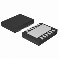
NCP5030MTTXG ON Semiconductor, NCP5030MTTXG Datasheet - Page 9

NCP5030MTTXG
Manufacturer Part Number
NCP5030MTTXG
Description
IC LED DRIVR HIGH BRIGHT 12-WDFN
Manufacturer
ON Semiconductor
Type
HBLED Driverr
Datasheet
1.NCP5030MTTXG.pdf
(14 pages)
Specifications of NCP5030MTTXG
Constant Current
Yes
Topology
PWM, Step-Down (Buck), Step-Up (Boost)
Number Of Outputs
1
Internal Driver
Yes
Type - Primary
Flash/Torch
Type - Secondary
White LED
Frequency
600kHz ~ 800kHz
Voltage - Supply
2.7 V ~ 5.5 V
Voltage - Output
2.2 V ~ 5.5 V
Mounting Type
Surface Mount
Package / Case
12-VFDFN Exposed Pad
Operating Temperature
-40°C ~ 85°C
Current - Output / Channel
900mA
Internal Switch(s)
Yes
Efficiency
87%
Operating Supply Voltage (typ)
3.3/5V
Number Of Segments
1
Operating Temperature (min)
-40C
Operating Temperature (max)
85C
Operating Temperature Classification
Industrial
Package Type
WDFN
Pin Count
12
Mounting
Surface Mount
Operating Supply Voltage (min)
2.7V
Operating Supply Voltage (max)
5.5V
Operating Supply Voltage
2.7 V to 5.5 V
Maximum Supply Current
5 mA
Maximum Operating Temperature
+ 85 C
Mounting Style
SMD/SMT
Minimum Operating Temperature
- 40 C
Lead Free Status / RoHS Status
Lead free / RoHS Compliant
Other names
NCP5030MTTXG
NCP5030MTTXGOSTR
NCP5030MTTXGOSTR
Available stocks
Company
Part Number
Manufacturer
Quantity
Price
Company:
Part Number:
NCP5030MTTXG
Manufacturer:
SHARP
Quantity:
1 000
Operation
Mode PWM architecture specifically designed to
efficiently provide a regulated current to a high current
white LED. This device utilizes fixed frequency
synchronous buck−boost switching regulator architecture.
This topology is critical in single cell Lithium−Ion/
Polymer battery or 3 Alkaline powered applications as the
forward voltage of the LED may be greater than or less than
the battery voltage. A low feedback voltage of 200 mV
(nom) minimizes power losses in the current setting
resistor connected between the cathode of the LED and
ground.
bridge with four low R
maximize efficient power delivery. Another advantage of
this topology is that it supports a true−shut down mode
where the LED will be disconnected from the power supply
when the device is placed in disable mode.
charge and discharge the current from P
through the inductor.
function of V
V
mode when V
nominal) and in Buck−Boost mode when V
this tow thresholds.
OUT
The NCP5030 DC−DC converter is based on a Current
The core switching regulator is configured as a full
Figure 16 shows how the four switches are connected to
The converter operates in three different modes as a
Figure 16. Basic Power Switches Topology
is below V
V
V
IN
IN
OUT
Figure 17. Conversion Mode
OUT
LX1
I
IN
IN
− V
– 650 mV (T
is above V
P1
N1
IN
Buck−Boost
DSON
2− Phase
3− Phase
2− Phase
(Figure 17): In Buck mode when
Boost
L
Buck
(0.1 W) MOSFET switches to
I
LX2
OUT
IN
P2
N2
BUCK
+ 375 mV (T
C
V
nominal), in Boost
V
OUT
OUT
OUT
OUT
T
T
VIN
BUCK
BOOST
is between
to V
http://onsemi.com
BOOST
OUT
9
to trigger the PWM controller on each rising edge (SET
signal) which starts a cycle. In pure buck or boost mode, the
converter operates in two−phase mode, the first one to
charge the inductor, followed by a synchronous rectifier
discharge phase. However, in buck−boost mode, to get high
efficiency the converter controls the switches in three
separate phases (see Buck−Boost Mode Section). The
capacitor C
smooth output voltage thus constantly powering the load.
Buck Mode (V
two others are fixed, the switch N2 is all time OFF and the
switch P2 is all time ON. The buck converter operates in
two separate phase (See Figure 18). The first one is T
when I
is OFF and the current increases through the inductor. The
switch current is measured by the SENSE CURRENT and
added to the RAMP COMP signal. Then PWM COMP
compares the output of the adder and the signal from
ERROR AMP. When the comparator threshold is
exceeded, T
turned OFF and N1 is ON until next clock rising edge. The
current is only delivered by the inductor, which means that
I
Boost Mode (V
in buck mode. Switches P2 and N2 are toggling and the two
others are fixed. Switch P1 is all time ON and the switch N1
is all time OFF. The boost converter operates in two
separate phases (See Figure 19). The first one is T
IN
The internal oscillator provides a 700 kHz clock signal
In Buck mode, switches P1 and N1 are toggling and the
The switches in boost mode are inversely controlled than
I
LX1
LX2
OUT
= 0
I
L
IN
Figure 18. Basic DC−DC Buck Operation
= I
OUT
OUT
ON
OUT
OUT
. During this phase the switch P1 is ON, N1
is used to store energy from the inductor to
phase is followed by T
Cycle
Start
T
< V
1.43 mS
> V
ON
IN
IN
– 650 mV)
+ 375 mV)
LX2 = V
T
OFF
OUT
OFF
. P1 switch is
ON
I
I
peak
valley
when
ON


