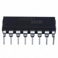
IR21571PBF International Rectifier, IR21571PBF Datasheet - Page 16

IR21571PBF
Manufacturer Part Number
IR21571PBF
Description
IC CONTROLLER BALLAST 16DIP
Manufacturer
International Rectifier
Type
Ballast Controllerr
Datasheet
1.IR21571PBF.pdf
(18 pages)
Specifications of IR21571PBF
Frequency
45.5 ~ 50.5 kHz
Current - Supply
5.5mA
Current - Output
500mA
Voltage - Supply
11.4 V ~ 15.6 V
Operating Temperature
-40°C ~ 125°C
Package / Case
16-DIP (0.300", 7.62mm)
Lead Free Status / RoHS Status
Lead free / RoHS Compliant
Other names
*IR21571PBF
A high voltage, fast recovery diode D
called bootstrap diode) is connected between V
(anode) and VB (cathode), and a capacitor C
(the so-called bootstrap capacitor) is connected
between the VB and VS leads. During half-bridge
switching, when MOSFET Q2 is on and Q1 is off, the
bootstrap capacitor C
decoupling capacitor, through the bootstrap diode
D
and Q1 is on, the bootstrap diode is reverse-biased,
and the bootstrap capacitor (which ‘floats’ on the
source of the upper power MOSFET) serves as the
IR21571 (S) & (PbF)
16
BOOT
VDC
CPH
RPH
RUN
RT
CT
DT
OC
Figure 19: Typical bootstrap supply connection
1
2
3
4
5
6
7
8
with V
, and through Q2. Alternately, when Q2 is off
CC
16
15
14
13
12
11
10
charge pump from half-bridge output
9
VCC
COM
HO
CS
SD
VS
VB
LO
(shaded area)
C
D
R
BOOT
BOOT
GHS
BOOT
AC line
rectifie
R
GLS
d
R
C
SUPPLY
R3
VCC
is charged from the V
D1
V
BUS
+V
BUS
return
Q1
Q2
R
CS
BOOT
C
D2
SNUBBER
1
/
2
(the so-
output
Bridge
BOOT
CC
CC
power supply to the upper gate driver CMOS circuitry.
Since the quiescent current in this CMOS circuitry is
very low (typically 45 A in the on-state), the majority
of the drop in the V
due to the transfer of charge from the bootstrap
capacitor to the gate of the power MOSFET.
VB should be bypassed to VS as close as possible to
the leads of the IC with a low ESR/ESL capacitor. A
PCB layout example is shown in figure 20. A rule of
thumb for the value of this capacitor is to keep its
minimum value at least 50 times the value of the total
input capacitance (Ciss) of the MOSFET or IGBT being
driven. In addition, the VS lead should be connected
directly to the high side power MOSFET source.
IR21571
Figure 20: Supply bypassing PCB layout example
pin 1
BS
C
voltage when Q1 is on occurs
VCC
(surface mount)
C
BOOT
C
(surface mount)
VCC
D
(through hole)
Boot
(surface mount)
www.irf.com


