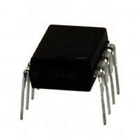
IRS2530DPBF International Rectifier, IRS2530DPBF Datasheet - Page 15

IRS2530DPBF
Manufacturer Part Number
IRS2530DPBF
Description
IC CTRL BALLAST DIMMING 8-DIP
Manufacturer
International Rectifier
Series
DIM8™r
Type
Ballast Controllerr
Datasheet
1.IRS2530DSTRPBF.pdf
(23 pages)
Specifications of IRS2530DPBF
Frequency
34.2 ~ 115 kHz
Current - Supply
5mA
Current - Output
260mA
Voltage - Supply
12.5 V ~ 15.6 V
Operating Temperature
-40°C ~ 125°C
Package / Case
8-DIP (0.300", 7.62mm)
Rohs Compliant
Yes
Peak Reflow Compatible (260 C)
Yes
Supply Current
5mA
Driver Case Style
DIP
No. Of Pins
8
Operating Temperature Range
-40°C To +125°C
Leaded Process Compatible
Yes
For Use With
IRPLDIM5E - KIT DES BALLAST 4LEVEL DIM FLUORIRPLDIM4E - KIT DES BALLAST 26W IRS2530DIRPLCFL8U - KIT DES FLUOR BALLAST IRS2530D
Lead Free Status / RoHS Status
Lead free / RoHS Compliant
Available stocks
Company
Part Number
Manufacturer
Quantity
Price
Company:
Part Number:
IRS2530DPBF
Manufacturer:
IR
Quantity:
3 825
Part Number:
IRS2530DPBF
Manufacturer:
IR
Quantity:
20 000
IRS2530D(S)
High-Q
Vout
Vin
Ignition
10%
50%
Start
100%
Low-Q
Frequency
fmin
f100%
f50%
f10%
fmax
Figure 4, Resonant tank Bode plot with lamp
dimming operating points.
Dim Mode
When the lamp ignites, the ballast output stage becomes a series-L, parallel-RC circuit and the AC lamp
current flows through the current sensing resistor, RCS. The resulting AC voltage across resistor RCS is
coupled to the DIM pin through feedback resistor, RFB (1 kΩ, typical), and feedback capacitor, CFB (0.1 μF,
typical). The DIM pin voltage is a combination of the DC offset voltage provided by the user dim setting and
the AC voltage that is capacitively coupled through capacitor CFB from the lamp current sensing resistor to
the DIM pin. The IC enters Dim Mode when the lamp ignites and the dimming control loop becomes active.
The DC+AC voltage at the DIM pin is regulated by the control loop such that the valley of the AC voltage
always stays at COM. By offsetting the AC voltage with a DC reference and holding the valley of the AC
voltage at COM, the amplitude of the AC voltage, and therefore the AC lamp current, is accurately controlled.
When the DC reference voltage at the DIM pin is decreased for dimming, the valleys of the AC voltage are
pushed below COM. The dimming control circuit increases the frequency to decrease the AC lamp current
until the AC valleys at the DIM pin are at COM again. When the DC reference is increased to increase the
brightness level, the valleys of the AC voltage increase above COM. The dimming control circuit decreases
the frequency to increase the AC lamp current until the AC valleys at the DIM pin are at COM again. In this
way, the dimming control circuit keeps the AC lamp current peak-to-peak amplitude regulated to the desired
value at all DC dim level settings. Capacitor CVCO programs the speed of the dimming loop and is typically
set to a low value (2.2 nF, typical) for cycle-by-cycle lamp current control. An additional compensation
network is formed by RVCO (1.5 kΩ, typical) and CPH to prevent the VCO voltage from changing too much
from one cycle to the next for maintaining smooth and stable dimming. A capacitor, CDIM (10 nF, typical) is
also necessary from the DIM pin to COM for filtering high-frequency switching noise.
During Dim Mode, the VS-sensing circuit and non-ZVS and crest factor protection circuits are also enabled
(see State Diagram, Page 11).
Non Zero-Voltage Switching (ZVS) Protection
During Dim Mode, if the voltage at the VS pin has not slewed entirely to COM during the dead-time such that
there is voltage between the drain and source of the external low-side half-bridge MOSFET when LO turns-
on, then the system is operating too close to, or, on the capacitive side of resonance. The result is non-ZVS
capacitive-mode switching that causes high peak currents to flow in the half-bridge MOSFETs that can
damage or destroy them (Figure 5). This can typically occur during a decrease of the DC bus during an AC
mains interrupt or brown-out condition, lamp variations over time, driving an incorrect lamp type, or
component and temperature variations. To protect against this, an internal high-voltage MOSFET is turned
on at each turn-off of HO and the VS-sensing circuit measures the VS voltage at each rising edge of LO. If
the VS voltage is greater than V
(4.5 V, typical), the non-ZVS control circuit will increase the frequency
ZVSTH
until ZVS is reached again. Increasing the frequency due to non-ZVS during a brown-out also ensures that
www.irf.com
© 2008 International Rectifier
15


