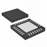
MAX8785AETI+T Maxim Integrated Products, MAX8785AETI+T Datasheet - Page 17

MAX8785AETI+T
Manufacturer Part Number
MAX8785AETI+T
Description
IC CCFL CTRL 28-TQFN
Manufacturer
Maxim Integrated Products
Type
CCFL Controllerr
Datasheet
1.MAX8785AETIT.pdf
(19 pages)
Specifications of MAX8785AETI+T
Current - Supply
1.5mA
Voltage - Supply
4.5 V ~ 28 V
Operating Temperature
-40°C ~ 85°C
Package / Case
28-TQFN Exposed Pad
Lead Free Status / RoHS Status
Lead free / RoHS Compliant
Current - Output
-
Frequency
-
Lead Free Status / Rohs Status
Details
The TFLT capacitor determines the delay time for both
open-lamp fault and arc fault. The MAX8785A charges
the TFLT capacitor with a 0.75µA current source during
open-lamp fault and charges the TFLT capacitor with a
2.8mA current source during an arc fault and sec-
ondary short circuit. The MAX8785A sets the fault latch
when the TFLT voltage reaches 3V. Use the following
equations to calculate the open-lamp fault delay
(t
cuit delay (t
The high-side gate drivers are powered using two boot-
strap circuits. The MAX8785A integrates the bootstrap
diodes so only two 0.1µF bootstrap capacitors are
needed. Connect the capacitors between LX1 and
BST1 and between LX2 and BST2 to complete the
bootstrap circuits.
Careful PC board layout is important to achieve stable
operation. The high-voltage sections and the switching
section of the circuit require particular attention. The
high-voltage sections of the layout need to be well sep-
arated from the control circuit. Follow these guidelines
for good PC board layout:
OPEN_LAMP
SHORT_CIRCUIT
t
), arc fault (t
SHORT CIRCUIT
t
OPEN LAMP
t
______________________________________________________________________________________
Setting the Fault Delay Time
ARC
_
_
=
ARC
C
):
TFLT
=
2 8
Bootstrap Capacitors
.
), and secondary short-cir-
C
=
mA
TFLT
0 75
C
×
.
Layout Guidelines
TFLT
2 8
3
.
V
μ
×
mA
A
3
×
V
3
V
Piezoelectric Transformers
Full-Bridge Controller for
1) Keep the high-current paths short and wide, espe-
2) Use a star ground configuration for power and ana-
3) Route high-speed switching nodes away from sen-
4) Mount the decoupling capacitor from V
5) The current-sense paths for LX to GND must be
6) Ensure the feedback connections are short and
7) To the extent possible, high-voltage trace clearance
cially at the ground terminals. This is essential for
stable, jitter-free operation and high efficiency.
log grounds. The power and analog grounds should
be completely isolated, meeting only at the center of
the star. The center should be placed at the analog
ground pin (GND).
sitive analog areas (V
and TFLT).
close as possible to the IC with dedicated traces that
are not shared with other signal paths.
made using Kelvin-sense connections to guarantee
the current-limit accuracy. With 8-pin SO MOSFETs,
this is best done by routing power to the MOSFETs
from outside using the top copper layer, while con-
necting GND and LX inside (underneath) the 8-pin
SO package.
direct. To the extent possible, IFB, VFB, and OLF
connections should be far away from the high-voltage
traces and the transformer.
on the transformer’s secondary should be widely
separated. The high-voltage traces should also be
separated from adjacent ground planes to prevent
lossy capacitive coupling.
CC
, RATE, HF, LF, COMP,
CC
to GND as
17


