SI8235BB-C-IS1 Silicon Laboratories Inc, SI8235BB-C-IS1 Datasheet - Page 12
SI8235BB-C-IS1
Manufacturer Part Number
SI8235BB-C-IS1
Description
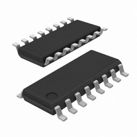
IC DUAL LOW SIDE DRIVER 16SOIC
Manufacturer
Silicon Laboratories Inc
Specifications of SI8235BB-C-IS1
Package / Case
16-SOIC (3.9mm Width)
Configuration
Low-Side
Input Type
Non-Inverting
Delay Time
60ns
Current - Peak
4A
Number Of Configurations
2
Number Of Outputs
2
Voltage - Supply
6.5 V ~ 24 V
Operating Temperature
-40°C ~ 125°C
Mounting Type
Surface Mount
Mounting Style
SMD/SMT
Number Of Channels
2
Propagation Delay Time
30 ns
Supply Voltage (max)
5.5 V
Supply Voltage (min)
4.5 V
Supply Current
2 mA
Power Dissipation
1.2 W
Maximum Operating Temperature
+ 125 C
Minimum Operating Temperature
- 40 C
Number Of Drivers
2
Driver Configuration
Non-Inverting
Input Logic Level
TTL
Rise Time
12ns
Fall Time
12ns
Frequency (max)
8MHz
Operating Supply Voltage (max)
5.5/24V
Peak Output Current
4A
Output Resistance
2.7Ohm
Operating Supply Voltage (min)
4.5/6.5V
Operating Temp Range
-40C to 125C
Operating Temperature Classification
Automotive
Mounting
Surface Mount
Pin Count
16
Package Type
SOIC N
Lead Free Status / RoHS Status
Lead free / RoHS Compliant
High Side Voltage - Max (bootstrap)
-
Lead Free Status / Rohs Status
Lead free / RoHS Compliant
Other names
336-1898-5
Available stocks
Company
Part Number
Manufacturer
Quantity
Price


Si823x
Table 4. Insulation and Safety-Related Specifications
Table 5. IEC 60664-1 (VDE 0884 Part 2) Ratings
12
Parameter
Nominal Air Gap
(Clearance)
Nominal External Tracking
(Creepage)
Minimum Internal Gap
(Internal Clearance)
Tracking Resistance
(Proof Tracking Index)
Erosion Depth
Resistance
(Input-Output)
Capacitance
(Input-Output)
Input Capacitance
Notes:
Parameter
Basic Isolation Group
Installation Classification
1. The values in this table correspond to the nominal creepage and clearance values as detailed in “7. Package Outline:
2. To determine resistance and capacitance, the Si823x is converted into a 2-terminal device. Pins 1–8 (1-7, 14 LD LGA)
3. Measured from input pin to ground.
16-Pin Wide Body SOIC” , “9. Package Outline: 16-Pin Narrow Body SOIC” , “11. Package Outline: 14 LD LGA
(5 x 5 mm)” , and “13. Package Outline: 14 LD LGA with Thermal Pad (5 x 5 mm)” . VDE certifies the clearance and
creepage limits as 4.7 mm minimum for the NB SOIC-16 and 8.5 mm minimum for the WB SOIC-16 package. UL does
not impose a clearance and creepage minimum for component level certifications. CSA certifies the clearance and
creepage limits as 3.9 mm minimum for the NB SOIC 16 and 7.6 mm minimum for the WB SOIC-16 package.
are shorted together to form the first terminal and pins 9–16 (8-14, 14 LD LGA) are shorted together to form the second
terminal. The parameters are then measured between these two terminals.
1
1
2
2
3
Symbol
L(1O1)
L(1O2)
Material Group
Rated Mains Voltages < 150 V
Rated Mains Voltages < 300 V
Rated Mains Voltages < 400 V
Rated Mains Voltages < 600 V
PTI
R
C
ED
C
IO
IO
I
Test Conditions
Condition
IEC60112
f = 1 MHz
Test
Rev. 1.1
WBSOIC-16
5 kV
0.014
0.040
10
600
8.0
8.0
1.4
4.0
RMS
RMS
RMS
RMS
RMS
12
WBSOIC-16
NBSOIC-16
SOIC-16
2.5 kV
8.0/4.01
8.0/4.01
WB
0.014
0.019
I-IV
I-IV
I-III
I-III
10
600
1.4
4.0
I
12
RMS
Value
SOIC-16
2.5 kV
NB
I-IV
I-III
Specification
I-II
I-II
I
14 LD
0.014
0.021
LGA
10
600
3.5
3.5
1.4
4.0
12
RMS
14 LD
LGA
I-IV
I-III
I-II
I-II
1.5 kV
I
LGA w/
14 LD
0.014
0.021
1.75
1.75
10
Pad
600
1.4
4.0
12
RMS
w/ Pad
14 LD
LGA
I-IV
I-III
I-II
I-I
I
Unit
mm
mm
mm
mm
pF
pF
V
Related parts for SI8235BB-C-IS1
Image
Part Number
Description
Manufacturer
Datasheet
Request
R

Part Number:
Description:
SOIC 16/A°/2.5KV 4A DUAL LOW SIDE ISOLATED DRIVER (ISODRIVER)
Manufacturer:
Silicon Laboratories Inc
Part Number:
Description:
SOIC 16/A°/2.5KV 4A DUAL LOW SIDE ISOLATED DRIVER (ISODRIVER)
Manufacturer:
Silicon Laboratories Inc

Part Number:
Description:
IC DUAL LOW SIDE DRIVER 16SOIC
Manufacturer:
Silicon Laboratories Inc
Datasheet:

Part Number:
Description:
IC ISODRIVER DUAL LOW SIDE 14LGA
Manufacturer:
Silicon Laboratories Inc
Datasheet:
Part Number:
Description:
IC ISODRIVER DUAL LOW SIDE 14LGA
Manufacturer:
Silicon Laboratories Inc
Datasheet:
Part Number:
Description:
4A DUAL LOW SIDE DRIVER
Manufacturer:
Silicon Laboratories Inc
Datasheet:

Part Number:
Description:
0.5 And 4.0 A Isodrivers
Manufacturer:
Silicon Laboratories
Datasheet:
Part Number:
Description:
SMD/C°/SINGLE-ENDED OUTPUT SILICON OSCILLATOR
Manufacturer:
Silicon Laboratories Inc
Part Number:
Description:
Manufacturer:
Silicon Laboratories Inc
Datasheet:
Part Number:
Description:
N/A N/A/SI4010 AES KEYFOB DEMO WITH LCD RX
Manufacturer:
Silicon Laboratories Inc
Datasheet:
Part Number:
Description:
N/A N/A/SI4010 SIMPLIFIED KEY FOB DEMO WITH LED RX
Manufacturer:
Silicon Laboratories Inc
Datasheet:
Part Number:
Description:
N/A/-40 TO 85 OC/EZLINK MODULE; F930/4432 HIGH BAND (REV E/B1)
Manufacturer:
Silicon Laboratories Inc
Part Number:
Description:
EZLink Module; F930/4432 Low Band (rev e/B1)
Manufacturer:
Silicon Laboratories Inc
Part Number:
Description:
I°/4460 10 DBM RADIO TEST CARD 434 MHZ
Manufacturer:
Silicon Laboratories Inc