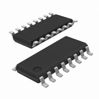
SI8235BB-C-IS1 Silicon Laboratories Inc, SI8235BB-C-IS1 Datasheet - Page 44

SI8235BB-C-IS1
Manufacturer Part Number
SI8235BB-C-IS1
Description
IC DUAL LOW SIDE DRIVER 16SOIC
Manufacturer
Silicon Laboratories Inc
Specifications of SI8235BB-C-IS1
Package / Case
16-SOIC (3.9mm Width)
Configuration
Low-Side
Input Type
Non-Inverting
Delay Time
60ns
Current - Peak
4A
Number Of Configurations
2
Number Of Outputs
2
Voltage - Supply
6.5 V ~ 24 V
Operating Temperature
-40°C ~ 125°C
Mounting Type
Surface Mount
Mounting Style
SMD/SMT
Number Of Channels
2
Propagation Delay Time
30 ns
Supply Voltage (max)
5.5 V
Supply Voltage (min)
4.5 V
Supply Current
2 mA
Power Dissipation
1.2 W
Maximum Operating Temperature
+ 125 C
Minimum Operating Temperature
- 40 C
Number Of Drivers
2
Driver Configuration
Non-Inverting
Input Logic Level
TTL
Rise Time
12ns
Fall Time
12ns
Frequency (max)
8MHz
Operating Supply Voltage (max)
5.5/24V
Peak Output Current
4A
Output Resistance
2.7Ohm
Operating Supply Voltage (min)
4.5/6.5V
Operating Temp Range
-40C to 125C
Operating Temperature Classification
Automotive
Mounting
Surface Mount
Pin Count
16
Package Type
SOIC N
Lead Free Status / RoHS Status
Lead free / RoHS Compliant
High Side Voltage - Max (bootstrap)
-
Lead Free Status / Rohs Status
Lead free / RoHS Compliant
Other names
336-1898-5
Available stocks
Company
Part Number
Manufacturer
Quantity
Price
Si823x
12. Land Pattern: 14 LD LGA
Figure 49 illustrates the recommended land pattern details for the Si823x in a 14-pin LGA. Table 23 lists the values
for the dimensions shown in the illustration.
44
Notes:
General:
Solder Mask Design:
Stencil Design:
Card Assembly:
1. All dimensions shown are in millimeters (mm).
2. This Land Pattern Design is based on the IPC-7351 guidelines.
3. All dimensions shown are at Maximum Material Condition (MMC). Least
4. All metal pads are to be non-solder mask defined (NSMD). Clearance
5. A stainless steel, laser-cut and electro-polished stencil with trapezoidal
6. The stencil thickness should be 0.125 mm (5 mils).
7. The ratio of stencil aperture to land pad size should be 1:1.
8. A No-Clean, Type-3 solder paste is recommended.
9. The recommended card reflow profile is per the JEDEC/IPC J-STD-020
Material Condition (LMC) is calculated based on a Fabrication
Allowance of 0.05 mm.
between the solder mask and the metal pad is to be 60 µm minimum, all
the way around the pad.
walls should be used to assure good solder paste release.
specification for Small Body Components.
Table 23. 14-Pin LGA Land Pattern Dimensions
Figure 49. 14-Pin LGA Land Pattern
Dimension
C1
X1
Y1
E
Rev. 1.1
(mm)
4.20
0.65
0.80
0.40


