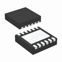
LTC4352CDD#TRPBF Linear Technology, LTC4352CDD#TRPBF Datasheet

LTC4352CDD#TRPBF
Specifications of LTC4352CDD#TRPBF
Available stocks
Related parts for LTC4352CDD#TRPBF
LTC4352CDD#TRPBF Summary of contents
Page 1
... A REV pin enables reverse current, overriding the diode behavior when desired. L, LT, LTC, LTM, Linear Technology and the Linear logo are registered trademarks and ThinSOT and PowerPath are trademarks of Linear Technology Corporation. All other trademarks are the property of their respective owners. ...
Page 2
... PLASTIC DFN T = 150°C, θ = 43°C/W JMAX JA EXPOSED PAD (PIN 13) PCB GND CONNECTION OPTIONAL orDer inForMaTion LEAD FREE FINISH TAPE AND REEL LTC4352CDD#PBF LTC4352CDD#TRPBF LTC4352IDD#PBF LTC4352IDD#TRPBF LTC4352HDD#PBF LTC4352HDD#TRPBF LTC4352CMS#PBF LTC4352CMS#TRPBF LTC4352IMS#PBF LTC4352IMS#TRPBF LTC4352HMS#PBF LTC4352HMS#TRPBF Consult LTC Marketing for parts specified with wider operating temperature ranges. *The temperature grade is identified by a label on the shipping container. ...
Page 3
T SYMBOL PARAMETER Supplies V Input Operating Range External Supply Range CC(EXT Internal Regulator Voltage CC(INT Supply Current External V ...
Page 4
LTC4352 Typical perForMance characTerisTics V Open, unless otherwise noted Current vs Voltage IN 1.6 1.2 0.8 0 (V) IN 4352 G01 OUT Current vs Voltage 300 250 200 150 100 ...
Page 5
FuncTions V (Pin 1): Voltage Sense and Supply Input. Connect this IN pin to the power input side of the MOSFET. The low voltage supply V is generated from V . The voltage sensed this pin ...
Page 6
LTC4352 FuncTional DiagraM CP4 – – + 2.57V CP3 – FAULT + CP2 0.5V – OV FAULT + OV 4 CP1 *DD PACKAGE ONLY CHARGE PUMP V ...
Page 7
The LTC4352 controls either single or back-to-back N-channel MOSFETs in order to emulate an ideal diode. Dual MOSFETs eliminate current flow from the input to the output in an input undervoltage or overvoltage condition. When enabled, an amplifier (AMP) ...
Page 8
LTC4352 applicaTions inForMaTion High availability systems often employ parallel-connected power supplies or battery feeds to achieve redundancy and enhance system reliability. ORing diodes have been a popular means of connecting these supplies at the point of load. Diodes with storage ...
Page 9
CPO and GATE Start-Up In single MOSFET applications, CPO is initially pulled diode below the SOURCE pin (Figure 3). In back-to- back MOSFET applications, CPO starts off at 0V, since SOURCE is near ground (Figure ...
Page 10
LTC4352 applicaTions inForMaTion Undervoltage and Overvoltage Protection Unlike a regular diode, the LTC4352 can prevent out of range input voltages from affecting the load voltage. This requires back-to-back MOSFETs, and resistive dividers from the input to the UV and OV ...
Page 11
External CPO Supply The internal charge pump takes milliseconds to charge up the CPO pin capacitor especially during device power up. This time can be shortened by connecting an external supply to the CPO pin. A series resistor ...
Page 12
LTC4352 applicaTions inForMaTion LEDs, D1 and D2, require around 3mA for good luminous intensity. Accounting for a 2V diode drop and 0. and R2 are set to 2.7k. PCB Layout Considerations Connect the V and OUT pin traces ...
Page 13
Typical applicaTions 12V GND BACKPLANE 3. 1N4148 OR BAT85 Plug-in Card Supply Holdup Using Ideal Diode at Input Q1 Si7336ADP HOT SWAP CONTROLLER SOURCE V GATE OUT IN LTC4352 GND CONNECTORS PLUG-IN CARD Ideal Diode with Reverse ...
Page 14
LTC4352 package DescripTion 0.70 ±0.05 2.38 ±0.05 3.50 ±0.05 2.10 ±0.05 1.65 ±0.05 PACKAGE OUTLINE 0.25 ± 0.05 0.45 BSC 2.25 REF RECOMMENDED SOLDER PAD PITCH AND DIMENSIONS APPLY SOLDER MASK TO AREAS THAT ARE NOT SOLDERED 0.889 ± 0.127 ...
Page 15
... Revised Typical Application and Related Parts list Information furnished by Linear Technology Corporation is believed to be accurate and reliable. However, no responsibility is assumed for its use. Linear Technology Corporation makes no representa- tion that the interconnection of its circuits as described herein will not infringe on existing patent rights. ...
Page 16
... Internal N-Channel 26.5V, TSSOP-16, DFN-14 Internal P-Channel, 2.6V to 5.5V, 40μA I P-Channel, 2.5V to 28V/36V, 11μA I Dual Internal P-Channel, 2.5V to 5.5V, DFN-10 P-Channel 36V, 30μA I www.linear.com ● TO LOAD , SOT- TSOT- MSOP MSOP-10 Q 4352fa LT 1210 REV A • PRINTED IN USA LINEAR TECHNOLOGY CORPORA TION 2008 ...


