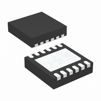
LTC4352CDD#TRPBF Linear Technology, LTC4352CDD#TRPBF Datasheet - Page 12

LTC4352CDD#TRPBF
Manufacturer Part Number
LTC4352CDD#TRPBF
Description
IC IDEAL DIODE CNTRL 12-DFN
Manufacturer
Linear Technology
Datasheet
1.LTC4352CMSPBF.pdf
(16 pages)
Specifications of LTC4352CDD#TRPBF
Applications
Redundant Power Supplies, Telecom Infrastructure
Fet Type
N-Channel
Number Of Outputs
1
Internal Switch(s)
No
Delay Time - On
250ns
Delay Time - Off
200ns
Voltage - Supply
2.9 V ~ 18 V
Current - Supply
1.4mA
Operating Temperature
0°C ~ 70°C
Mounting Type
Surface Mount
Package / Case
12-DFN
Lead Free Status / RoHS Status
Lead free / RoHS Compliant
Available stocks
Company
Part Number
Manufacturer
Quantity
Price
applicaTions inForMaTion
LEDs, D1 and D2, require around 3mA for good luminous
intensity. Accounting for a 2V diode drop and 0.5V V
R1 and R2 are set to 2.7k.
PCB Layout Considerations
Connect the V
to the MOSFET’s terminals. Keep the traces to the MOSFET
wide and short to minimize resistive losses. The PCB traces
LTC4352
12
IN
and OUT pin traces as close as possible
FROM INPUT
SUPPLY
TRACK WIDTH W:
0.03˝ PER AMPERE
ON 1OZ CU FOIL
Figure 8. Recommended PCB Layout for Power MOSFET
CURRENT FLOW
W
S
S
S
G
DRAWING IS NOT TO SCALE!
C1
OL
,
SO-8
LTC4352
Q1
associated with the power path through the MOSFET should
have low resistance. See Figure 8.
It is also important to put C1, the bypass capacitor for the
V
place C2 near the CPO and SOURCE pins. Surge suppres-
sors, when used, should be mounted close to the LTC4352
using short lead lengths.
CC
VIA TO GROUND PLANE
pin, as close as possible between V
D
D
D
D
MSOP-12
CURRENT FLOW
VIA TO GROUND PLANE
W
TO LOAD
4352 F08
CC
and GND. Also
4352fa


