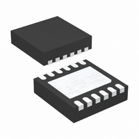
LTC4352CDD#TRPBF Linear Technology, LTC4352CDD#TRPBF Datasheet - Page 9

LTC4352CDD#TRPBF
Manufacturer Part Number
LTC4352CDD#TRPBF
Description
IC IDEAL DIODE CNTRL 12-DFN
Manufacturer
Linear Technology
Datasheet
1.LTC4352CMSPBF.pdf
(16 pages)
Specifications of LTC4352CDD#TRPBF
Applications
Redundant Power Supplies, Telecom Infrastructure
Fet Type
N-Channel
Number Of Outputs
1
Internal Switch(s)
No
Delay Time - On
250ns
Delay Time - Off
200ns
Voltage - Supply
2.9 V ~ 18 V
Current - Supply
1.4mA
Operating Temperature
0°C ~ 70°C
Mounting Type
Surface Mount
Package / Case
12-DFN
Lead Free Status / RoHS Status
Lead free / RoHS Compliant
Available stocks
Company
Part Number
Manufacturer
Quantity
Price
applicaTions inForMaTion
CPO and GATE Start-Up
In single MOSFET applications, CPO is initially pulled up
to a diode below the SOURCE pin (Figure 3). In back-to-
back MOSFET applications, CPO starts off at 0V, since
SOURCE is near ground (Figure 4). CPO starts ramping
up 10µs after V
Another 40µs later, GATE will also start ramping up with
CPO if UV, OV and V
ramp rate is decided by the CPO pull-up current into the
combined CPO and GATE pin capacitances. An internal
clamp limits the CPO voltage to 6.7V above SOURCE,
while the final GATE voltage is determined by the forward
drop servo amplifier.
MOSFET Selection
The LTC4352 drives N-channel MOSFETs to conduct the
load current. The important features of the MOSFET are
its threshold voltage, the maximum drain-source voltage
BV
The gate drive for the MOSFET is guaranteed to be between
5V and 7.5V. This allows the use of logic level threshold
Figure 3. Start-up Waveform for Single MOSFET Application
DSS
VOLTAGE
(5V/DIV)
, and the on-resistance R
V
C2 = 0.1µF
IN
= 5V
CC
clears its undervoltage lockout level.
IN
– OUT conditions allow it to. The
TIME (2.5ms/DIV)
CPO
V
GATE
OUT
V CC
DS(ON)
IN
, SOURCE
.
4352 FO3
N-channel MOSFETs. The maximum allowable drain-source
voltage, BV
as the full supply voltage can appear across the MOSFET
when the input falls to 0V.
The FAULT pin pulls low to signal an open MOSFET fault
whenever the forward voltage drop across the enhanced
MOSFET exceeds 250mV. The R
enough to conduct the maximum load current while not
triggering such a fault (when using FAULT), and to stay
within the MOSFET’s power rating at the maximum load
current.
CPO Capacitor Selection
The recommended value of the capacitor between the
CPO and SOURCE pins is approximately 10x the input
capacitance, C
a correspondingly longer time to charge up by the internal
charge pump. A smaller capacitor suffers more voltage
drop during a fast gate turn-on event as it shares charge
with the MOSFET gate capacitance.
Figure 4. Start-up Waveform for Back-to-Back MOSFET Application
VOLTAGE
(5V/DIV)
DSS
V
C2 = 0.1µF
ISS
IN
, must be higher than the supply voltages
= 5V
, of the MOSFET. A larger capacitor takes
TIME (2.5ms/DIV)
CPO
GATE
OUT
V CC
DS(ON)
V
IN
LTC4352
should be small
4352 FO4
4352fa
9


