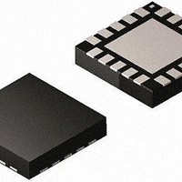
MAX16922ATPA/V+ Maxim Integrated Products, MAX16922ATPA/V+ Datasheet - Page 13

MAX16922ATPA/V+
Manufacturer Part Number
MAX16922ATPA/V+
Description
IC DCDC CONV STPDN DL LDO 20WQFN
Manufacturer
Maxim Integrated Products
Datasheet
1.MAX16922ATPAVT.pdf
(17 pages)
Specifications of MAX16922ATPA/V+
Applications
General Purpose
Current - Supply
5µA
Operating Temperature
-40°C ~ 125°C
Mounting Type
Surface Mount
Package / Case
20-WQFN Exposed Pad, 20-DQFN
Output Voltage
1 V, 2.7 V, 3.3 V, 5 V
Output Current
450 mA, 600 mA, 1.2 A
Switching Frequency
2.2 MHz
Input / Supply Voltage (max)
28 V
Input / Supply Voltage (min)
3.7 V
Maximum Operating Temperature
+ 125 C
Mounting Style
SMD/SMT
Duty Cycle (max)
100 %
Load Regulation
+/- 0.2 %
Minimum Operating Temperature
- 40 C
Number Of Outputs
4
Operating Temperature Range
- 40 C to + 125 C
Supply Current
14 uA
Lead Free Status / RoHS Status
Lead free / RoHS Compliant
Voltage - Supply
-
Lead Free Status / Rohs Status
Lead free / RoHS Compliant
When the EN input is pulled high and PV1 is greater
than 3.7V (typ), the 5V LSUP linear regulator turns on.
Once LSUP exceeds 2.5V, the internal reference and
bias are enabled. When the internal bias has stabilized
OUT1, soft-start is initiated. After completion of soft-start
on OUT1 (2.8ms typ), OUT2 soft-start is initiated. OUT3
soft-start is enabled when PV3 is greater than or equal
to 1.25V (typ), and OUT4 soft-start is enabled when PV4
is greater than or equal to 1.5V (typ).
Care must be taken when driving the EN pin. Digital
input signals deliver a fast edge that is properly detect-
ed by the MAX16922. If driving the EN pin with an ana-
log voltage that has a slew rate of less than 1V/ms or a
voltage-divider from PV1, then the input voltage on PV1
must always be less than 6V when the voltage at EN is
near the turn-off threshold of 1.6V. If this cannot be
guaranteed, then a 1kΩ resistor or 5.6V zener diode
must be placed in parallel with the LSUP output capaci-
tor to prevent possible damage to the device.
The MAX16922 can be shut down by thermal shut-
down, enable low (EN), LSUP regulator undervoltage,
Power-Down and Restart Sequence
VBAT
Applications Information
______________________________________________________________________________________
0.1μF
Power-On Sequence
Converters, Dual LDOs, and RESET
220μF
2.2MHz, Dual, Step-Down DC-DC
V
4.7μF
4.7μF
OUT2
4.7μF
4.7μF
V
4.7μF
OUT1
PV1
EN
PWM
PV3
OUT3
GND1
GND3
PV4
OUT4
GND
GND2
or when PV1 falls below 3.0V (typ). When a shutdown
occurs, all outputs discharge through an internal resis-
tor connected between each output and ground. When
enable is high, the die temperature is okay, the LSUP
linear regulator is greater than 2.5V (typ), and OUT1 is
less than 1.25V (typ); a complete soft-start power-on
sequence is reinitiated.
The OUT1 step-down converter operates with a 4.7µH
inductor and the OUT2 step-down converter operates
with a 2.2µH inductor. The inductor’s DC current rating
must be high enough to account for peak ripple current
and load transients. The step-down converter’s archi-
tecture has minimal current overshoot during startup
and load transients. In most cases, an inductor capable
of 1.3 times the maximum load current is acceptable.
For optimum performance choose an inductor with DC-
series resistance in the 50mΩ to 150mΩ range. For
higher efficiency at heavy loads (above 400mA) and
minimal load regulation, the inductor resistance should
be kept as small as possible. For light-load applications
(up to 200mA), higher resistance is acceptable with
very little impact on performance.
MAX16922
EP
Typical Applications Circuit
PGND2
OUTS2
OUTS1
RESET
LSUP
LX2
PV2
BST
LX1
2.2μH
0.1μF
4.7μF
4.7μH
1μF
V
OUT1
20kΩ
Inductor Selection
10μF
V
OUT2
10μF
V
OUT1
13


