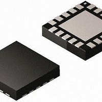
MAX16922ATPA/V+ Maxim Integrated Products, MAX16922ATPA/V+ Datasheet - Page 15

MAX16922ATPA/V+
Manufacturer Part Number
MAX16922ATPA/V+
Description
IC DCDC CONV STPDN DL LDO 20WQFN
Manufacturer
Maxim Integrated Products
Datasheet
1.MAX16922ATPAVT.pdf
(17 pages)
Specifications of MAX16922ATPA/V+
Applications
General Purpose
Current - Supply
5µA
Operating Temperature
-40°C ~ 125°C
Mounting Type
Surface Mount
Package / Case
20-WQFN Exposed Pad, 20-DQFN
Output Voltage
1 V, 2.7 V, 3.3 V, 5 V
Output Current
450 mA, 600 mA, 1.2 A
Switching Frequency
2.2 MHz
Input / Supply Voltage (max)
28 V
Input / Supply Voltage (min)
3.7 V
Maximum Operating Temperature
+ 125 C
Mounting Style
SMD/SMT
Duty Cycle (max)
100 %
Load Regulation
+/- 0.2 %
Minimum Operating Temperature
- 40 C
Number Of Outputs
4
Operating Temperature Range
- 40 C to + 125 C
Supply Current
14 uA
Lead Free Status / RoHS Status
Lead free / RoHS Compliant
Voltage - Supply
-
Lead Free Status / Rohs Status
Lead free / RoHS Compliant
High-switching frequencies and relatively large peak
currents make PCB layout a very important aspect of
design. Good design minimizes excessive EMI on the
feedback paths and voltage gradients in the ground
plane, both of which can result in instability or regula-
tion errors. Connect the input capacitors as close as
possible to the PV_ and ground. Connect the inductor
and output capacitors as close as possible to the
device and keep the traces short, direct, and wide to
minimize the current loop area.
* Other standard versions may be available. Contact factory for availability.
NUMBER
SUFFIX*
PART
G
A
B
C
D
E
H
F
J
I
VOLTAGE
OUT1
5.00
5.00
5.00
5.00
5.00
3.30
3.30
3.30
3.80
______________________________________________________________________________________
(V)
3.6
MAX16922 AUP x
VOLTAGE
MAX16922 ATP x /V +
Converters, Dual LDOs, and RESET
OUT2
2.70
1.20
3.30
3.30
1.20
1.20
1.20
3.30
1.2
(V)
Off
2.2MHz, Dual, Step-Down DC-DC
PCB Layout
VOLTAGE
/V +
OUT3
2.80
3.30
1.80
1.20
2.50
3.15
2.50
2.85
2.50
3.3
(V)
LEAD FREE
AEC Q100 QUALIFIED
OUTPUT VOLTAGES RESET THRESHOLD, RESET TIMEOUT
-40°C TO +125°C OPERATION, TQFN, 20 PINS
LEAD FREE
AEC Q100 QUALIFIED
OUTPUT VOLTAGES RESET THRESHOLD, RESET TIMEOUT
-40°C TO +125°C OPERATION, TSSOP, 20 PINS
VOLTAGE
The OUTS_ feedback connections are sensitive to
inductor magnetic field interference so route these
traces away from the inductors and noisy traces such
as LX_.
Connect GND_ and PGND2 to the ground plane.
Connect the exposed paddle to the ground plane
with multiple vias to help conduct heat away from
the device.
Refer to the MAX16922 evaluation kit for a PCB layout
example.
OUT4
1.80
3.00
1.80
1.80
1.80
1.20
(V)
1.0
3.3
3.0
3.3
OUT1 RESET
THRESHOLD
(%)
90
90
90
90
90
90
90
90
90
90
TIMEOUT
RESET
(ms)
14.9
14.9
14.9
14.9
14.9
14.9
14.9
14.9
14.9
14.9
Selector Guide
REFRESH
ENABLE
LOAD
BST
On
On
On
Off
On
On
On
Off
Off
Off
15


