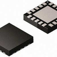
MAX16922ATPA/V+ Maxim Integrated Products, MAX16922ATPA/V+ Datasheet - Page 14

MAX16922ATPA/V+
Manufacturer Part Number
MAX16922ATPA/V+
Description
IC DCDC CONV STPDN DL LDO 20WQFN
Manufacturer
Maxim Integrated Products
Datasheet
1.MAX16922ATPAVT.pdf
(17 pages)
Specifications of MAX16922ATPA/V+
Applications
General Purpose
Current - Supply
5µA
Operating Temperature
-40°C ~ 125°C
Mounting Type
Surface Mount
Package / Case
20-WQFN Exposed Pad, 20-DQFN
Output Voltage
1 V, 2.7 V, 3.3 V, 5 V
Output Current
450 mA, 600 mA, 1.2 A
Switching Frequency
2.2 MHz
Input / Supply Voltage (max)
28 V
Input / Supply Voltage (min)
3.7 V
Maximum Operating Temperature
+ 125 C
Mounting Style
SMD/SMT
Duty Cycle (max)
100 %
Load Regulation
+/- 0.2 %
Minimum Operating Temperature
- 40 C
Number Of Outputs
4
Operating Temperature Range
- 40 C to + 125 C
Supply Current
14 uA
Lead Free Status / RoHS Status
Lead free / RoHS Compliant
Voltage - Supply
-
Lead Free Status / Rohs Status
Lead free / RoHS Compliant
2.2MHz, Dual, Step-Down DC-DC
Converters, Dual LDOs, and RESET
The input capacitor, CIN1, reduces the current peaks
drawn from the supply and reduces switching noise in
the MAX16922. The impedance of CIN1 at the switch-
ing frequency should be kept very low. Ceramic capac-
itors with X5R or X7R dielectrics are recommended due
to their small size, low ESR, and small temperature
coefficients. Use a 4.7µF ceramic capacitor or an
equivalent amount of multiple capacitors in parallel
between PV1 and ground. Connect CIN1 as close to
the device as possible to minimize the impact of PCB
trace inductance.
Connect a minimum 4.7µF ceramic capacitor between
PV2 to ground, and a 2.2µF ceramic capacitor between
PV3 to ground and PV4 to ground. Since PV2 is cas-
caded from OUT1, the input capacitor connected to
PV2 can be used as part of the total output capacitance
for OUT1.
The step-down output capacitors are required to keep
the output-voltage ripple small and to ensure regulation
loop stability. These capacitors must have low imped-
ance at the switching frequency. Surface-mount ceram-
ic capacitors are recommended due to their small size
and low ESR. The capacitor should maintain its
capacitance overtemperature and DC bias. Ceramic
capacitors with X5R or X7R temperature characteristics
generally perform well. The output capacitance can be
very low. Place a minimum of 15µF ceramic capaci-
tance from OUTS1 to ground and a minimum of 10µF
from OUTS2 to ground. When the OUT2 output voltage
selection is below 2.35V, the output capacitance should
be increased to prevent instability. For optimum load-
transient performance and very low output ripple, the
output capacitance can be increased. The maximum
output capacitance should not exceed 3.8mF for OUT1
and 2.0mF for OUT2.
Connect a 4.7µF ceramic capacitor between OUT3 and
GND, and a second 4.7µF ceramic capacitor from
OUT4 to GND. When the input voltage of an LDO is
greater than 2.35V, the output capacitor can be
decreased to 2.2µF. The equivalent series resistance
14
______________________________________________________________________________________
LDO Output Capacitors and Stability
Step-Down Output Capacitors
Capacitor Selection
Input Capacitors
(ESR) of the LDO output capacitors affects stability and
output noise. Use output capacitors with an ESR of
0.1Ω or less to ensure stable operation and optimum
transient response. Connect these capacitors as close
as possible to the device to minimize PCB trace induc-
tance.
The maximum package power dissipation of the
MAX16922 in the 20-pin thin QFN package is 2500mW.
The power dissipated by the MAX16922 should not
exceed this rating. The total device power dissipation is
the sum of the power dissipation of the four regulators:
Estimate the OUT1 and OUT2 power dissipations as
follows:
where η is the efficiency (see the Typical Operating
Characteristics section).
Calculate the OUT3 and OUT4 power dissipations as
follows:
The maximum junction temperature of the MAX16922 is
+150°C. The junction-to-case thermal resistance (θ
of the MAX16922 is 2.7°C/W.
When mounted on a single-layer PCB, the junction to
ambient thermal resistance (θ
48°C/W. Mounted on a multilayer PCB, θ
mately 32°C/W. Calculate the junction temperature of
the MAX16922 as follows:
where T
sure the calculated value of T
+150°C maximum.
A
is the maximum ambient temperature. Make
P
P
P
P
D3
D4
P
D
D
D
= P
2
1
= I
= I
=
=
T
J
I
I
OUT3
OUT4
D1
OUT
OUT
= T
+ P
1
2
Thermal Considerations
A
×
x (V
x (V
×
D2
x P
V
V
OUT
OUT
PV3
PV4
+ P
D
x θ
J
1
2
D3
JA
×
– V
– V
does not exceed the
×
JA
1
) is approximately
1
+ P
−
η
OUT3
OUT4
−
η
η
η
D4
JA
)
)
is approxi-
JC
)


