MAX8588ETM+ Maxim Integrated Products, MAX8588ETM+ Datasheet - Page 18
MAX8588ETM+
Manufacturer Part Number
MAX8588ETM+
Description
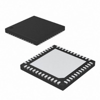
IC PMIC HI EFF LOW IQ 48-TQFN
Manufacturer
Maxim Integrated Products
Type
Low-IQ PMICr
Datasheet
1.MAX8588ETMT.pdf
(31 pages)
Specifications of MAX8588ETM+
Applications
Processor
Voltage - Supply
2.6 V ~ 5.5 V
Operating Temperature
-40°C ~ 85°C
Mounting Type
Surface Mount
Package / Case
48-TQFN Exposed Pad
Output Voltage Range
1.2375 V to 1.2625 V
Input Voltage Range
2.4 V to 5.5 V
Input Current
32 uA
Power Dissipation
2105 mW
Operating Temperature Range
- 40 C to + 85 C
Mounting Style
SMD/SMT
Input Voltage
5.5V
No. Of Outputs
1
Power Dissipation Pd
2.105W
Supply Voltage Range
2.6V To 5.5V
No. Of Pins
48
Filter Terminals
SMD
Rohs Compliant
Yes
Frequency
1MHz
Lead Free Status / RoHS Status
Lead free / RoHS Compliant
Current - Supply
-
Lead Free Status / Rohs Status
Lead free / RoHS Compliant


High-Efficiency, Low-I
Dynamic Core for PDAs and Smartphones
The MAX8588 power-management IC is optimized for
devices using Intel X-Scale microprocessors, including
third-generation smart cell phones, PDAs, internet
appliances, and other portable devices requiring sub-
stantial computing and multimedia capability at low
power. The MAX8588 complies with Intel Processor
Power specifications.
The IC integrates seven high-performance, low-operat-
ing-current power supplies along with supervisory and
management functions. Regulator outputs include three
step-down DC-DC outputs (V1, V2, and V3), three lin-
ear regulators (V4, V5, and V6), and one always-on out-
put, V7 (Intel VCC_BATT). The V1 step-down DC-DC
converter provides 3.3V or adjustable output voltage for
I/O and peripherals. The V2 step-down DC-DC convert-
er is preset for 3.3V or 2.5V. V2 can also be adjusted
with external resistors on all parts. The V3 step-down
DC-DC converter provides a serial-programmed output
for powering microprocessor cores. The three linear
regulators (V4, V5, and V6) provide power for PLL,
SRAM, and USIM.
To minimize sleep-state quiescent current, V1 and V2
have bypass “sleep” LDOs that can be activated to
minimize battery drain when output current is very low.
Other functions include separate on/off control for all
DC-DC converters, low-battery and dead-battery
detection, a power-OK output, a backup-battery input,
and a two-wire serial interface.
All DC-DC outputs use fast, 1MHz PWM switching and
small external components. They operate with fixed-fre-
quency PWM control and automatically switch from
PWM to skip-mode operation at light loads to reduce
operating current and extend battery life. The V3 core
output is capable of forced-PWM operation at all loads.
The 2.6V to 5.5V input voltage range allows 1-cell Li+,
3-cell NiMH, or a regulated 5V input.
The following power-supply descriptions include the
Intel terms for the various voltages in parenthesis. For
example, the V1 output is referred to as VCC_IO in Intel
documentation. See Figure 1.
V1 is a 1MHz current-mode step-down converter. The V1
output voltage can be preset to 3.3V or adjusted using a
resistor voltage-divider. V1 supplies loads up to 1300mA.
Idle Mode is a trademark of Maxim Integrated Products, Inc.
18
______________________________________________________________________________________
V1 and V2 (VCC_IO, VCC_MEM)
Step-Down DC-DC Converters
Detailed Description
Q
PMIC with
V2 is also a 1MHz current-mode step-down converter.
The V2 step-down DC-DC converter is preset for 3.3V
or 2.5V. V2 can also be adjusted with external resistors
on all parts. V2 supplies loads up to 900mA.
Under moderate to heavy loading, the converters operate
in a low-noise PWM mode with constant frequency and
modulated pulse width. Switching harmonics generated
by fixed-frequency operation are consistent and easily fil-
tered. Efficiency is enhanced under light loading (<30mA
typ), by assuming an Idle Mode™ during which the con-
verter switches only as needed to service the load.
Internal n-channel synchronous rectifiers eliminate the
need for external Schottky diodes and improve efficien-
cy. The synchronous rectifier turns on during the sec-
ond half of each cycle (off-time). During this time, the
voltage across the inductor is reversed, and the induc-
tor current falls. In normal operation (not forced PWM),
the synchronous rectifier turns off at the end of the
cycle (at which time another on-time begins) or when
the inductor current approaches zero.
If the inductor current does not rise sufficiently to sup-
ply the load during the on-time, the switch remains on,
allowing operation up to 100% duty cycle. This allows
the output voltage to maintain regulation while the input
voltage approaches the regulation voltage. Dropout
voltage is approximately 180mV for an 800mA load on
V1 and 220mV for an 800mA load on V2. During
dropout, the high-side p-channel MOSFET turns on,
and the controller enters a low-current-consumption
mode. The device remains in this mode until the regula-
tor channel is no longer in dropout.
In addition to the high-efficiency step-down converters,
V1 and V2 can also be supplied with low-quiescent cur-
rent, low-dropout (LDO) linear regulators that can be
used in sleep mode or at any time when the load current
is very low. The sleep LDOs can source up to 35mA. To
enable the sleep LDOs, drive SLP low. When SLP is high,
the switching step-down converters are active. The out-
put voltage of the sleep LDOs is set to be the same as
the switching step-down converters as described in the
Setting the Output Voltages section. SLPIN is the input to
the V1 and V2 sleep LDOs and must connect to IN.
100% Duty-Cycle Operation
Synchronous Rectification
Sleep LDOs
Related parts for MAX8588ETM+
Image
Part Number
Description
Manufacturer
Datasheet
Request
R

Part Number:
Description:
High-Efficiency Low-IQ PMIC
Manufacturer:
Maxim Integrated Products
Datasheet:
Part Number:
Description:
Manufacturer:
Maxim Integrated Products
Datasheet:
Part Number:
Description:
MAX7528KCWPMaxim Integrated Products [CMOS Dual 8-Bit Buffered Multiplying DACs]
Manufacturer:
Maxim Integrated Products
Datasheet:
Part Number:
Description:
Single +5V, fully integrated, 1.25Gbps laser diode driver.
Manufacturer:
Maxim Integrated Products
Datasheet:
Part Number:
Description:
Single +5V, fully integrated, 155Mbps laser diode driver.
Manufacturer:
Maxim Integrated Products
Datasheet:
Part Number:
Description:
VRD11/VRD10, K8 Rev F 2/3/4-Phase PWM Controllers with Integrated Dual MOSFET Drivers
Manufacturer:
Maxim Integrated Products
Datasheet:
Part Number:
Description:
Highly Integrated Level 2 SMBus Battery Chargers
Manufacturer:
Maxim Integrated Products
Datasheet:
Part Number:
Description:
Current Monitor and Accumulator with Integrated Sense Resistor; ; Temperature Range: -40°C to +85°C
Manufacturer:
Maxim Integrated Products
Part Number:
Description:
TSSOP 14/A°/RS-485 Transceivers with Integrated 100O/120O Termination Resis
Manufacturer:
Maxim Integrated Products
Part Number:
Description:
TSSOP 14/A°/RS-485 Transceivers with Integrated 100O/120O Termination Resis
Manufacturer:
Maxim Integrated Products
Part Number:
Description:
QFN 16/A°/AC-DC and DC-DC Peak-Current-Mode Converters with Integrated Step
Manufacturer:
Maxim Integrated Products
Part Number:
Description:
TDFN/A/65V, 1A, 600KHZ, SYNCHRONOUS STEP-DOWN REGULATOR WITH INTEGRATED SWI
Manufacturer:
Maxim Integrated Products
Part Number:
Description:
Integrated Temperature Controller f
Manufacturer:
Maxim Integrated Products
Part Number:
Description:
SOT23-6/I°/45MHz to 650MHz, Integrated IF VCOs with Differential Output
Manufacturer:
Maxim Integrated Products
Part Number:
Description:
SOT23-6/I°/45MHz to 650MHz, Integrated IF VCOs with Differential Output
Manufacturer:
Maxim Integrated Products