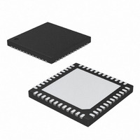
MAX8588ETM+ Maxim Integrated Products, MAX8588ETM+ Datasheet - Page 23

MAX8588ETM+
Manufacturer Part Number
MAX8588ETM+
Description
IC PMIC HI EFF LOW IQ 48-TQFN
Manufacturer
Maxim Integrated Products
Type
Low-IQ PMICr
Datasheet
1.MAX8588ETMT.pdf
(31 pages)
Specifications of MAX8588ETM+
Applications
Processor
Voltage - Supply
2.6 V ~ 5.5 V
Operating Temperature
-40°C ~ 85°C
Mounting Type
Surface Mount
Package / Case
48-TQFN Exposed Pad
Output Voltage Range
1.2375 V to 1.2625 V
Input Voltage Range
2.4 V to 5.5 V
Input Current
32 uA
Power Dissipation
2105 mW
Operating Temperature Range
- 40 C to + 85 C
Mounting Style
SMD/SMT
Input Voltage
5.5V
No. Of Outputs
1
Power Dissipation Pd
2.105W
Supply Voltage Range
2.6V To 5.5V
No. Of Pins
48
Filter Terminals
SMD
Rohs Compliant
Yes
Frequency
1MHz
Lead Free Status / RoHS Status
Lead free / RoHS Compliant
Current - Supply
-
Lead Free Status / Rohs Status
Lead free / RoHS Compliant
One data bit is transferred during each SCL clock
cycle. The data on SDA must remain stable during the
high period of the SCL clock pulse. Changes in SDA
while SCL is high are control signals (see the START
and STOP Conditions section). Both SDA and SCL idle
high when the bus is not busy.
When the serial interface is inactive, SDA and SCL idle
high. A master device initiates communication by issu-
ing a START condition. A START condition is a high-to-
low transition on SDA with SCL high. A STOP condition
is a low-to-high transition on SDA while SCL is high
(Figure 5). A START condition from the master signals
the beginning of a transmission to the MAX8588. The
master terminates transmission by issuing a not
acknowledge followed by a STOP condition (see the
Acknowledge Bit section). The STOP condition frees
the bus.
When a STOP condition or incorrect address is detect-
ed, the MAX8588 internally disconnects SCL from the
serial interface until the next START condition, minimiz-
ing digital noise and feedthrough.
The acknowledge bit (ACK) is the ninth bit attached to
every 8-bit data word. The receiving device always
generates ACK. The MAX8588 generates an ACK when
receiving an address or data by pulling SDA low during
the ninth clock period. Monitoring ACK allows for
detection of unsuccessful data transfers. An unsuc-
cessful data transfer occurs if a receiving device is
busy or if a system fault has occurred. In the event of
an unsuccessful data transfer, the bus master should
reattempt communication at a later time.
Figure 5. I
A = START CONDITION
B = MSB OF ADDRESS CLOCKED INTO SLAVE
C = LSB OF ADDRESS CLOCKED INTO SLAVE
D = R/W BIT CLOCKED INTO SLAVE
E = SLAVE PULLS SMB DATA LINE LOW
SCL
SDA
2
C-Compatible Serial-Interface Timing Diagram
t
SU:STA
Dynamic Core for PDAs and Smartphones
A
t
HD:STA
______________________________________________________________________________________
START and STOP Conditions
t
LOW
B
t
HIGH
Acknowledge Bit (ACK)
High-Efficiency, Low-I
t
SU:DAT
C
Bit Transfer
F = ACKNOWLEDGE BIT CLOCKED INTO MASTER
G = MSB OF DATA CLOCKED INTO SLAVE (OP/SUS BIT)
H = LSB OF DATA CLOCKED INTO SLAVE
I = SLAVE PULLS SMB DATA LINE LOW
D
E
F
A bus master initiates communication with a slave
device by issuing a START condition followed by the
7-bit slave address (Table 3). When idle, the MAX8588
waits for a START condition followed by its slave
address. The serial interface compares each address
value bit by bit, allowing the interface to power down
immediately if an incorrect address is detected.
The LSB of the address word is the read/write (R/W) bit.
R/W indicates whether the master is writing or reading
(RD/W 0 = write, RD/W 1 = read). The MAX8588 only
supports the SEND BYTE format; therefore, RD/W is
required to be 0.
After receiving the proper address, the MAX8588
issues an ACK by pulling SDA low for one clock cycle.
The MAX8588 has two user-programmed addresses
(Table 3). Address bits A6 through A1 are fixed, while
A1 is controlled by SRAD. Connecting SRAD to GND
sets A1 = 0. Connecting ADD to IN sets A1 = 1.
When V3 is dynamically changed with the serial inter-
face, the output voltage changes at a rate controlled by
a capacitor (C
The voltage change is a conventional RC exponential
described by:
Table 3. Serial Address
SRAD
t
HD:DAT
0
1
Vo(t) = Vo(0) + dV(1 – exp(-t / (100kΩ C
G
A7
0
0
RAMP
A6
0
0
H
) connected from RAMP to ground.
J = ACKNOWLEDGE CLOCKED INTO MASTER
K = ACKNOWLEDGE CLOCK PULSE
L = STOP CONDITION, DATA EXECUTED BY SLAVE
M = NEW START CONDITION
A5
1
1
V3 Output Ramp-Rate Control
I
Q
A4
0
0
J
PMIC with
A3
1
1
K
A2
t
0
0
SU:STO
Serial Address
L
RAMP
t
BUF
A1
0
1
M
)))
RD/W
A0
0
0
23


