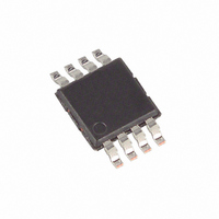
DS1825U+ Maxim Integrated Products, DS1825U+ Datasheet - Page 17

DS1825U+
Manufacturer Part Number
DS1825U+
Description
IC THERMOMETER DIGITAL 8-USOP
Manufacturer
Maxim Integrated Products
Datasheet
1.DS1825U.pdf
(21 pages)
Specifications of DS1825U+
Function
Thermometer, Thermostat
Topology
Register Bank, Scratchpad
Sensor Type
Internal
Sensing Temperature
-55°C ~ 125°C
Output Type
Digital
Output Alarm
Yes
Output Fan
No
Voltage - Supply
3 V ~ 3.7 V
Operating Temperature
-55°C ~ 125°C
Mounting Type
Surface Mount
Package / Case
8-MSOP, Micro8™, 8-uMAX, 8-uSOP,
Temperature Threshold
Programmable
Full Temp Accuracy
+/- 0.5 C
Digital Output - Bus Interface
1-Wire
Digital Output - Number Of Bits
9 bit to 12 bit
Supply Voltage (max)
3.7 V
Supply Voltage (min)
3 V
Maximum Operating Temperature
+ 125 C
Minimum Operating Temperature
- 55 C
Supply Current
1.5 mA
Ic Output Type
Digital
Sensing Accuracy Range
± 0.5°C
Supply Voltage Range
3V To 3.7V
Resolution (bits)
12bit
Sensor Case Style
µSOP
No. Of Pins
8
Accuracy %
0.5°C
Rohs Compliant
Yes
Lead Free Status / RoHS Status
Lead free / RoHS Compliant
Figure 15. READ/WRITE TIME SLOT TIMING DIAGRAM
READ TIME SLOTS
The DS1825 can only transmit data to the master when the master issues read time slots. Therefore, the master
must generate read time slots immediately after issuing a Read Scratchpad [BEh] or Read Power Supply [B4h]
command, so that the DS1825 can provide the requested data. In addition, the master can generate read time slots
after issuing Convert T [44h] or Recall E
the DS1825 FUNCTION COMMAND section.
All read time slots must be a minimum of 60ms in duration with a minimum of a 1ms recovery time between slots. A
read time slot is initiated by the master device pulling the 1-Wire bus low for a minimum of 1ms and then releasing
the bus (see Figure 14). After the master initiates the read time slot, the DS1825 will begin transmitting a 1 or 0 on
bus. The DS1825 transmits a 1 by leaving the bus high and transmits a 0 by pulling the bus low. When transmitting
a 0, the DS1825 will release the bus by the end of the time slot, and the bus will be pulled back to its high idle state
by the pullup resister. Output data from the DS1825 is valid for 15ms after the falling edge that initiated the read
time slot. Therefore, the master must release the bus and then sample the bus state within 15ms from the start of
the slot.
Figure 15 illustrates that the sum of T
shows that system timing margin is maximized by keeping T
master sample time during read time slots towards the end of the 15ms period.
1-WIRE BUS
1-WIRE BUS
V
GND
V
GND
PU
PU
> 1 ms
OF SLOT
START
15 ms
15 ms
LINE TYPE LEGEND
MASTER WRITE “0” SLOT
MASTER READ “0” SLOT
60 ms < T
MIN
Master samples
15 ms
Bus master pulling low
Resistor pullup
DS1825 Samples
INIT
X
“0” < 120 ms
TYP
, T
2
[B8h] commands to find out the status of the operation as explained in
45 ms
RC
, and T
30 ms
SAMPLE
17 of 21
MAX
> 1 ms
must be less than 15ms for a read time slot. Figure 16
INIT
OF SLOT
START
and T
DS1825 pulling low
15 ms
15 ms
RC
1 ms < T
1 ms < T
as short as possible and by locating the
MASTER WRITE “1” SLOT
> 1 ms
MASTER READ “1” SLOT
REC
REC
MIN
<
<
Master samples
¥
15 ms
¥
DS1825 Samples
TYP
30 ms
MAX


