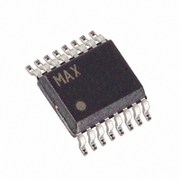
MAX8554EEE+ Maxim Integrated Products, MAX8554EEE+ Datasheet - Page 11

MAX8554EEE+
Manufacturer Part Number
MAX8554EEE+
Description
IC CNTRLR BUCK PWM 16-QSOP
Manufacturer
Maxim Integrated Products
Datasheet
1.MAX8553EEE.pdf
(24 pages)
Specifications of MAX8554EEE+
Pwm Type
Controller
Number Of Outputs
1
Frequency - Max
550kHz
Duty Cycle
95%
Voltage - Supply
4.5 V ~ 28 V
Buck
Yes
Boost
No
Flyback
No
Inverting
No
Doubler
No
Divider
Yes
Cuk
No
Isolated
No
Operating Temperature
-40°C ~ 85°C
Package / Case
16-QSOP
Frequency-max
550kHz
Output Voltage
0.6 V to 3.5 V
Output Current
25000 mA
Mounting Style
SMD/SMT
Switching Frequency
550 KHz
Maximum Operating Temperature
+ 85 C
Minimum Operating Temperature
- 40 C
Synchronous Pin
No
Topology
Buck
Dc
0649
Lead Free Status / RoHS Status
Lead free / RoHS Compliant
4.5V to 28V Input, Synchronous PWM Buck Controllers
PIN
10
11
12
13
14
15
16
1
2
3
4
5
6
7
8
9
for DDR Termination and Point-of-Load Applications
MAX8553
EN/HSD
REFIN
PGND
FSEL
VTTR
GND
POK
ILIM
REF
BST
VTT
DH
V+
DL
VL
LX
—
—
—
—
______________________________________________________________________________________
MAX8554
PGND
FSEL
GND
HSD
POK
OUT
ILIM
REF
BST
EN
DH
FB
V+
DL
VL
LX
—
—
—
—
Enable/High-Side Drain. Connect to the high-side N-channel MOSFET drain through a 5.1kΩ
resistor for normal operation. Connect to GND for low-power shutdown (Figure 2). If the enable
function is not used, connect EN/HSD directly to the high-side N-channel MOSFET drain.
High-Side Drain. Connect to the high-side N-channel MOSFET drain for normal operation.
Reference Input. An applied voltage at REFIN sets V
range is from 0 to +3.6V.
Enable. Drive EN high to enable the output. Drive EN low to shut down the IC. If the enable
function is not used, connect EN to V+.
Power-OK Output. POK is an open-drain output and is logic high when both VTT and VTTR are
within 12% of regulation. POK is pulled low in shutdown.
VTT Feedback Input. Connect to VTT output.
Output Feedback. Connect to the center of a resistor-divider between the output and ground to
set the output voltage. FB threshold is 0.6V.
Current-Limit Threshold Adjustment. Connect a resistor from ILIM to GND to set the current-limit
threshold, or connect ILIM to VL for the default setting. See the Setting the Current Limit section.
Frequency Select. Selects the switching frequency. See Tables 1 and 2 for configuration of
FSEL.
Reference. Connect a 0.22µF or greater capacitor from REF to GND.
Ground
VTTR Reference Output. Connect a 1µF or greater capacitor from VTTR to GND. VTTR is
capable of sourcing and sinking up to 25mA.
Output Voltage. Connect directly to the output. OUT senses the output voltage to determine the
on-time for the high-side switching MOSFET.
Input Supply Voltage. Supply input for the VL regulator. Bypass with a 0.22µF or greater
capacitor.
Internal Regulator Output. Connect a 2.2µF or greater capacitor from VL to GND. VL can be
connected to V+ if the operating range is from +4.5V to +5.5V.
Low-Side MOSFET Gate Drive. Connect to the gate of the low-side N-channel MOSFET. DL is
low in shutdown or in undervoltage lockout.
Power Ground
Bootstrapped Supply. Drives high-side N-channel MOSFET. Connect a 0.1µF or greater
capacitor from BST to LX.
High-Side MOSFET Gate Drive. Connect to the high-side N-channel MOSFET gate. DH is low in
shutdown or in undervoltage lockout.
Inductor Switching Node
FUNCTION
VTT
and V
VTTR
to 1/2 V
Pin Description
REFIN
. REFIN voltage
11


