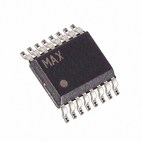
MAX8554EEE+ Maxim Integrated Products, MAX8554EEE+ Datasheet - Page 5

MAX8554EEE+
Manufacturer Part Number
MAX8554EEE+
Description
IC CNTRLR BUCK PWM 16-QSOP
Manufacturer
Maxim Integrated Products
Datasheet
1.MAX8553EEE.pdf
(24 pages)
Specifications of MAX8554EEE+
Pwm Type
Controller
Number Of Outputs
1
Frequency - Max
550kHz
Duty Cycle
95%
Voltage - Supply
4.5 V ~ 28 V
Buck
Yes
Boost
No
Flyback
No
Inverting
No
Doubler
No
Divider
Yes
Cuk
No
Isolated
No
Operating Temperature
-40°C ~ 85°C
Package / Case
16-QSOP
Frequency-max
550kHz
Output Voltage
0.6 V to 3.5 V
Output Current
25000 mA
Mounting Style
SMD/SMT
Switching Frequency
550 KHz
Maximum Operating Temperature
+ 85 C
Minimum Operating Temperature
- 40 C
Synchronous Pin
No
Topology
Buck
Dc
0649
Lead Free Status / RoHS Status
Lead free / RoHS Compliant
ELECTRICAL CHARACTERISTICS (continued)
(V
PGND = LX = GND, BST = VL, T
ELECTRICAL CHARACTERISTICS
(V
= LX = POK = GND, BST = VL, T
4.5V to 28V Input, Synchronous PWM Buck Controllers
POWER-OK OUTPUT
Upper VTT and VTTR Threshold
Lower VTT and VTTR Threshold
Upper Threshold
Lower Threshold
POK Output Low Level
POK Output High Leakage
V+ Input Voltage Range
V+ Input Voltage Range
EN/HSD Input Voltage Range
EN Input Voltage Range
EN Input Current
HSD Input Voltage Range
HSD Input Current
REFIN Input Voltage Range
V+ Supply Current (MAX8553)
V+ Supply Current (MAX8554)
REFIN Supply Current
EN/HSD Supply Current
VL Supply Current
V+ Shutdown Supply Current
REFIN Shutdown Supply Current
VL Shutdown Supply Current
VL Undervoltage-Lockout Threshold
VTT
VTT Input Bias Current
VTT Feedback Voltage Range
VTT Feedback Voltage Accuracy
FB Input Bias Current
FB Regulation Voltage
Output Adjust Range
V+
V+
= V
= V
for DDR Termination and Point-of-Load Applications
HSD
HSD
PARAMETER
PARAMETER
= +12V, V
= +12V, V
_______________________________________________________________________________________
EN/HSD
EN/HSD
= V
= V
A
A
REFIN
= 0°C to +85°C. Typical values are at T
= -40°C to +85°C, unless otherwise specified.) (Note 3)
REFIN
MAX8553
MAX8553
MAX8554
MAX8554
I
V
VL not connected to V+
VL connected to V+
MAX8553 enabled
MAX8554 enabled
MAX8554 enabled
V
V
V
EN/HSD = GND
EN/HSD = GND
V
Rising edge, typical hysteresis = 40mV
V
V
V
MAX8554, V
MAX8554, V
MAX8554 (Note 1)
SINK
= +2.5V, V
POK
VTT
FB
VL
VL
VTT
REFIN
REFIN
= +2.5V, V
= V
= V
= 630mV
= +1.35V
= +1.25V
= 2mA
= +5V
= V
= V
V+
V+
= 5.5V, V
= +5.5V, V
EN/HSD
EN/HSD
EN
FB
OUT
EN
= +5V, C
= +600mV
= +2.5V, FSEL unconnected
= +5V, C
= +1.8V
= +3.6V
VTT
CONDITIONS
CONDITIONS
EN/HSD
= +1.35V
VL
VL
= 4.7µF, C
= 0V
= 4.7µF, C
A
= +25°C, unless otherwise specified.)
VTTR
VTTR
= 1µF, C
= 1µF, C
REF
REF
= 0.22µF, V
0.646
0.504
0.598
MIN
4.05
49.5
49.5
MIN
-0.2
-0.2
4.5
1.5
1.5
1.5
0.6
55
43
= 0.22µF, V
6
0
0
0.672
0.528
FSEL
TYP
56
44
FSEL
= 0, ILIM = VL, PGND
0.698
0.552
0.616
MAX
MAX
= 0V, ILIM = VL,
28.0
28.0
28.0
0.90
4.40
50.5
50.5
250
0.4
5.5
3.6
1.2
1.2
1.8
3.5
57
45
28
40
10
12
5
3
5
1
0
0
% V
% V
% V
UNITS
UNITS
mA
mA
mA
µA
µA
µA
µA
µA
µA
µA
µA
µA
µA
RE FIN
RE FIN
V
V
V
V
V
V
V
V
V
V
V
RE FIN
V
V
5


