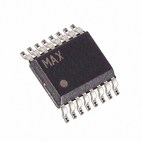
MAX8554EEE+ Maxim Integrated Products, MAX8554EEE+ Datasheet - Page 21

MAX8554EEE+
Manufacturer Part Number
MAX8554EEE+
Description
IC CNTRLR BUCK PWM 16-QSOP
Manufacturer
Maxim Integrated Products
Datasheet
1.MAX8553EEE.pdf
(24 pages)
Specifications of MAX8554EEE+
Pwm Type
Controller
Number Of Outputs
1
Frequency - Max
550kHz
Duty Cycle
95%
Voltage - Supply
4.5 V ~ 28 V
Buck
Yes
Boost
No
Flyback
No
Inverting
No
Doubler
No
Divider
Yes
Cuk
No
Isolated
No
Operating Temperature
-40°C ~ 85°C
Package / Case
16-QSOP
Frequency-max
550kHz
Output Voltage
0.6 V to 3.5 V
Output Current
25000 mA
Mounting Style
SMD/SMT
Switching Frequency
550 KHz
Maximum Operating Temperature
+ 85 C
Minimum Operating Temperature
- 40 C
Synchronous Pin
No
Topology
Buck
Dc
0649
Lead Free Status / RoHS Status
Lead free / RoHS Compliant
The droop resistor, R
the output inductor before the output capacitor, sets the
droop voltage, V
voltage at the maximum load current, including ripple, is
just above the lower limit of the output tolerance:
R
given by:
R
The MAX8553/MAX8554 drive external, logic-level, N-
channel MOSFETs as the circuit-switch elements. The
key selection parameters are:
On-resistance (R
Maximum drain-to-source voltage (V
should be at least 20% higher than the input supply rail
at the high-side MOSFET’s drain.
Gate charges (Q
4.5V to 28V Input, Synchronous PWM Buck Controllers
Figure
switching frequency.
DRP
DRP
R
should be chosen to handle this power dissipation.
SDN
6. A resistor-divider (R1 and R2) is used to lower the
introduces some power dissipation, which is
DRP
for DDR Termination and Point-of-Load Applications
10kΩ
R6
<
P
D DRP
2N7002
V
(
OUT TYP
DRP
Q3
G
DS(ON)
______________________________________________________________________________________
, Q
)
(
Setting Voltage Positioning
. Choose R
=
DRP
GD
R2
Power MOSFET Selection
R
)
DRP
, Q
-
): The lower, the better.
(R4) in
V
I
OUT MAX
OUT MIN
GS
×
): The lower, the better.
(
I
POK
V+
REFIN
EN/HSD
REF
ILIM
FSEL
GND
DRP
(
(
OUT MAX
Figure
)
(
R1
such that the output
MAX8553
)
-
V
RIPPLE
2, in series with
)
)
2
DSS
VIN
PGND
VTTR
BST
VTT
DH
DL
VL
LX
/
): This
2
Choose the MOSFETs with rated R
For a good compromise between efficiency and cost,
choose the high-side MOSFET that has a conduction
loss equal to switching loss at nominal input voltage and
maximum output current (see below). For the low-side
MOSFET, make sure that it does not spuriously turn on
because of the dV/dt caused by the high-side MOSFET
turning on, as this would result in shoot-through current
degrading the efficiency. MOSFETs with a lower Q
Q
For proper thermal-management design, calculate the
power dissipation at the desired maximum operating
junction temperature, maximum output current, and
worst-case input voltage (for low-side MOSFET, worst
case is at V
either at V
and low-side MOSFET have different loss components
due to the circuit operation. The low-side MOSFET
operates as a zero voltage switch; therefore, major
losses are: the channel conduction loss (P
body-diode conduction loss (P
drive loss (P
Use R
where V
the dead time (~30ns), and f
Because of the zero-voltage switch operation, low-side
MOSFET gate-drive loss occurs as a result of charging
and discharging the input capacitance (C
is distributed among the average DL gate driver’s
pullup and pulldown resistance, R
internal gate resistance (R
The drive power dissipated is given by:
The high-side MOSFET operates as a duty-cycle con-
trol switch and has the following major losses: the
channel conduction loss (P
switching loss (P
The high-side MOSFET does not have body-diode con-
duction loss because the diode never conducts current.
GS
P
ratio have higher immunity to dV/dt.
LSDR
DS(ON)
P
F
LSCC
is the body-diode forward-voltage drop, t
IN(MIN)
=
P
IN(MAX)
LSDR
LSDC
at T
C
=
ISS
):
J(MAX):
1
HSSW
or V
= ×
-
×
; for high-side MOSFET, it could be
2
V
OUT
V
(
V
IN(MAX)
IN
I
GS
LOAD
), and the drive loss (P
×
GATE
)
2
S
HSCC
×
(
×
is the switching frequency.
). The high-side MOSFET
I
LOAD
V
f
) of the MOSFET (~2Ω).
S
F
LSDC
×
DS(ON)
×
), the VI overlapping
DL
t
)
DT
R
2
GATE
×
), and the gate-
(~1.2Ω), and the
×
R
R
DS ON
f
at V
S
GATE
ISS
(
+
). This loss
LSCC
GS
R
)
DL
= 4.5V.
HSDR
), the
GD
DT
21
to
is
).


