ISL6265AHRTZ Intersil, ISL6265AHRTZ Datasheet - Page 12
ISL6265AHRTZ
Manufacturer Part Number
ISL6265AHRTZ
Description
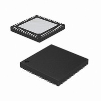
IC CTRLR MULTI-OUTPUT 48-TQFN
Manufacturer
Intersil
Datasheet
1.ISL6265AHRTZ.pdf
(23 pages)
Specifications of ISL6265AHRTZ
Applications
Controller, AMD SVI Capable Mobile
Voltage - Input
5 ~ 24 V
Number Of Outputs
3
Voltage - Output
0.5 ~ 1.55 V
Operating Temperature
-10°C ~ 100°C
Mounting Type
Surface Mount
Package / Case
48-TQFN
Lead Free Status / RoHS Status
Lead free / RoHS Compliant
Available stocks
Company
Part Number
Manufacturer
Quantity
Price
Company:

Part Number:
ISL6265AHRTZ
Manufacturer:
Intersil
Quantity:
800
Company:
Part Number:
ISL6265AHRTZ
Manufacturer:
INTERSIL
Quantity:
1 000
Part Number:
ISL6265AHRTZ
Manufacturer:
INTERSIL
Quantity:
20 000
Company:
Part Number:
ISL6265AHRTZ-T
Manufacturer:
HONEYWELL
Quantity:
100
Part Number:
ISL6265AHRTZ-T
Manufacturer:
INTERSIL
Quantity:
20 000


open the CPU Core1 negative sense and connect the RTN1
pin to a pull-up resistor.
Mode Selection
The OFS/VFIXEN pin selects between the AMD defined
VFIX and SVI modes of operation and enables droop if
desired in SVI mode only. If OFS/VFIXEN is tied to VCC,
then SVI mode with no droop on the core output(s) is
selected. Connected to +3.3V, VFIX mode is active with no
droop on the core output(s). SVI mode with droop is enabled
when OFS/VFIXEN is tied to ground through a resistor sized
to set the core voltage positive offset. Further information is
provided in “Offset Resistor Selection” on page 17.
Serial VID Interface
The on-board Serial VID Interface (SVI) circuitry allows the
processor to directly control the Core and Northbridge voltage
reference levels within the ISL6265A. The SVC and SVD
states are decoded according to the PWROK and VFIXEN
inputs as described in the following sections. The ISL6265A
uses a digital-to-analog converter (DAC) to generate a
reference voltage based on the decoded SVI value. See
Figure 7 for a simple SVI interface timing diagram.
VDD AND VDDNB
Interval 1 to 2: ISL6265A waits to POR.
Interval 2 to 3: SVC and SVD are externally set to pre-Metal VID code.
Interval 3 to 4: EN locks core output configuration and pre-Metal VID code. All outputs soft-start to this level.
Interval 4 to 5: PGOOD signal goes HIGH indicating proper operation.
Interval 5 to 6: CPU detects VDDPWRGD high and drives PWROK high to allow ISL6265A to prepare for SVI code.
Interval 6 to 7: SVC and SVD data lines communicate change in VID code.
Interval 7 to 8: ISL6265A responds to VID-ON-THE-FLY code change.
Interval 8 to 9: PWROK is driven low and ISL6265A returns all outputs to pre-PWROK Metal VID level.
Interval 9 to 10: PWROK driven high once again by CPU and ISL6265A prepares for SVI code.
Interval 10 to 11: SVC and SVD data lines communicate new VID code.
Interval 11 to 12: ISL6265A drives outputs to new VID code level.
Post 12 : Enable falls and all internal drivers are tri-stated and PGOOD is driven low.
VDDPWRGD
(PGOOD)
ENABLE
PWROK
FIXEN
VCC
SVC
SVD
FIGURE 7. SVI INTERFACE TIMING DIAGRAM: TYPICAL PRE-PWROK METAL VID STARTUP
1
12
2
3
METAL_VID
4
5
ISL6265A
6
Pre-PWROK Metal VID
Assuming the OFS/VFIXEN pin is not tied to +3.3V during
controller configuration, typical motherboard start-up begins
with the controller decoding the SVC and SVD inputs to
determine the pre-PWROK metal VID setting (see Table 1).
Once the enable input (EN) exceeds the rising enable
threshold, the ISL6265A decodes and locks the decoded
value in an on-board hold register.
The internal DAC circuitry begins to ramp Core and
Northbridge planes to the decoded pre-PWROK metal VID
output level. The digital soft-start circuitry ramps the internal
reference to the target gradually at a fixed rate of
approximately 2mV/µs. The controlled ramp of all output
7
V_SVI
SVC
0
0
1
1
TABLE 1. PRE-PWROK METAL VID CODES
8
METAL_VID
SVD
9
0
1
0
1
10
11
OUTPUT VOLTAGE (V)
V_SVI
12
1.1
1.0
0.9
0.8
May 11, 2009
FN6884.0
Related parts for ISL6265AHRTZ
Image
Part Number
Description
Manufacturer
Datasheet
Request
R

Part Number:
Description:
Multi-output Controller With Integrated Mosfet Drivers For Amd Svi Capable Mobile Cpus
Manufacturer:
Intersil Corporation
Datasheet:
Part Number:
Description:
Multi-Output Controller
Manufacturer:
Intersil Corporation
Datasheet:
Part Number:
Description:
Intersil Corporation [CMOS Serial Controller Interface]
Manufacturer:
Intersil Corporation
Datasheet:
Part Number:
Description:
Manufacturer:
Intersil Corporation
Datasheet:
Part Number:
Description:
357-036-542-201 CARDEDGE 36POS DL .156 BLK LOPRO
Manufacturer:
Intersil Corporation
Datasheet:
Part Number:
Description:
1024-Word x 4-Bit LSI Static RAM
Manufacturer:
Intersil Corporation
Datasheet:
Part Number:
Description:
General Purpose NPN Transistor Arrays FN341.4
Manufacturer:
Intersil Corporation
Datasheet:
Part Number:
Description:
CMOS 16-Bit Microprocessor
Manufacturer:
Intersil Corporation
Datasheet:
Part Number:
Description:
Manufacturer:
Intersil Corporation
Datasheet:
Part Number:
Description:
Manufacturer:
Intersil Corporation
Datasheet:
Part Number:
Description:
Manufacturer:
Intersil Corporation
Datasheet:
Part Number:
Description:
Manufacturer:
Intersil Corporation
Datasheet:
Part Number:
Description:
CMOS 6-Bit Latch and Decoder Memory Interfaces
Manufacturer:
Intersil Corporation
Datasheet:
Part Number:
Description:
CA3046General Purpose NPN Transistor Arrays
Manufacturer:
Intersil Corporation
Datasheet:
Part Number:
Description:
Manufacturer:
Intersil Corporation
Datasheet: