ISL6265AHRTZ Intersil, ISL6265AHRTZ Datasheet - Page 15
ISL6265AHRTZ
Manufacturer Part Number
ISL6265AHRTZ
Description
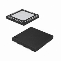
IC CTRLR MULTI-OUTPUT 48-TQFN
Manufacturer
Intersil
Datasheet
1.ISL6265AHRTZ.pdf
(23 pages)
Specifications of ISL6265AHRTZ
Applications
Controller, AMD SVI Capable Mobile
Voltage - Input
5 ~ 24 V
Number Of Outputs
3
Voltage - Output
0.5 ~ 1.55 V
Operating Temperature
-10°C ~ 100°C
Mounting Type
Surface Mount
Package / Case
48-TQFN
Lead Free Status / RoHS Status
Lead free / RoHS Compliant
Available stocks
Company
Part Number
Manufacturer
Quantity
Price
Company:

Part Number:
ISL6265AHRTZ
Manufacturer:
Intersil
Quantity:
800
Company:
Part Number:
ISL6265AHRTZ
Manufacturer:
INTERSIL
Quantity:
1 000
Part Number:
ISL6265AHRTZ
Manufacturer:
INTERSIL
Quantity:
20 000
Company:
Part Number:
ISL6265AHRTZ-T
Manufacturer:
HONEYWELL
Quantity:
100
Part Number:
ISL6265AHRTZ-T
Manufacturer:
INTERSIL
Quantity:
20 000


SVI Bus Protocol
The AMD processor bus protocol is compliant with SMBus
send byte protocol for VID transactions (see Figure 8). During a
send byte transaction, the processor sends the start sequence
followed by the slave address of the VR for which the VID
command applies. The address byte must be configured
according to Table 4. The processor then sends the write bit.
After the write bit, if the ISL6265A receives a valid address
byte, it sends the acknowledge bit. The processor then sends
the PSI-L bit and VID bits during the data phase. The Serial VID
8-bit data field encoding is outlined in Table 5. If ISL6265A
receives a valid 8-bit code during the data phase, it sends the
acknowledge bit. Finally, the processor sends the stop
sequence. After the ISL6265A has detected the stop, it can
then proceed with the VID-on-the-fly transition.
Operation
After the start-up sequence, the ISL6265A begins regulating
the core and Northbridge output voltages to the pre-PWROK
metal VID programmed. The controller monitors SVI
commands to determine when to enter power-savings mode,
BITS
BITS
6:0
6:4 Always 110b
7
3
2
1
0
TABLE 5. SERIAL VID 8-BIT DATA FIELD ENCODING
TABLE 4. SVI SEND BYTE ADDRESS DESCRIPTION
Reserved by AMD for future use
VDD1, if set then the following data byte contains the VID for
VDD1
VDD0, if set then the following data byte contains the VID for
VID0
VDDNB, if set then the following data byte contains the VID
for VIDNB
PSI_L:
= 0 means the processor is at an optimal load for the
regulator(s) to enter power-savings mode
= 1 means the processor is not at an optimal load for the
regulator(s) to enter power-saving mode
SVID[6:0] as defined in Table 3.
SVD
SVC
6
DESCRIPTION
DESCRIPTION
15
SLAVE ADDRESS PHASE
5
4
3
2
FIGURE 8. SEND BYTE EXAMPLE
1
0
ISL6265A
7
implement dynamic VID changes, and shutdown individual
outputs.
The ISL6265A controls the no-load output voltage of core and
Northbridge output to an accuracy of ±0.5% over-the-range of
0.75V to 1.5V. A fully differential amplifier implements core
voltage sensing for precise voltage control at the
microprocessor die.
Switching Frequency
The R
architecture. The switching frequency increases during the
application of a load to improve transient performance. It
also varies slightly due to changes in input and output
voltage and output current. This variation is normally less
than 10% in continuous conduction mode.
CORE FREQUENCY SELECTION
A resistor connected between the VW and COMP pins of the
Core segment of the ISL6265A adjusts the switching window
and therefore adjusts the switching frequency. The R
resistor that sets up the switching frequency of the converter
operating in CCM can be determined using Equation 3,
where R
Designs for 300kHz switching frequency would result in a
R
In discontinuous conduction mode (DCM), the ISL6265A
runs in period stretching mode.
NORTHBRIDGE FREQUENCY SELECTION
The Northbridge switching frequency to programmed by a
resistor connected from the FSET_NB pin to the GND pin.
The approximate PWM switching frequency is written as
shown in Equation 4:
Estimating the value of R
Equation 5:
Where F
the programming resistor and K = 1.5 x 10
R
F
R
FSET
SW
FSET
FSET
6
=
3
value of 6.81kΩ.
(
kΩ
modulator scheme is a variable frequency PWM
-----------------------------------
K R
=
FSET
5
SW
⋅
-------------------- -
K F
)
DATA PHASE
⋅
is the PWM switching frequency, R
FSETNB
=
(See Table 3)
1
1
4
is in kΩ and the switching period is in ms.
SW
(
Period μs
SVID
3
(
2
FSET_NB
) 0.4
–
1
)
×
0
2.33
is written as shown in
-10
.
FSET_NB
May 11, 2009
FSET
FN6884.0
(EQ. 3)
(EQ. 5)
(EQ. 4)
is
Related parts for ISL6265AHRTZ
Image
Part Number
Description
Manufacturer
Datasheet
Request
R

Part Number:
Description:
Multi-output Controller With Integrated Mosfet Drivers For Amd Svi Capable Mobile Cpus
Manufacturer:
Intersil Corporation
Datasheet:
Part Number:
Description:
Multi-Output Controller
Manufacturer:
Intersil Corporation
Datasheet:
Part Number:
Description:
Intersil Corporation [CMOS Serial Controller Interface]
Manufacturer:
Intersil Corporation
Datasheet:
Part Number:
Description:
Manufacturer:
Intersil Corporation
Datasheet:
Part Number:
Description:
357-036-542-201 CARDEDGE 36POS DL .156 BLK LOPRO
Manufacturer:
Intersil Corporation
Datasheet:
Part Number:
Description:
1024-Word x 4-Bit LSI Static RAM
Manufacturer:
Intersil Corporation
Datasheet:
Part Number:
Description:
General Purpose NPN Transistor Arrays FN341.4
Manufacturer:
Intersil Corporation
Datasheet:
Part Number:
Description:
CMOS 16-Bit Microprocessor
Manufacturer:
Intersil Corporation
Datasheet:
Part Number:
Description:
Manufacturer:
Intersil Corporation
Datasheet:
Part Number:
Description:
Manufacturer:
Intersil Corporation
Datasheet:
Part Number:
Description:
Manufacturer:
Intersil Corporation
Datasheet:
Part Number:
Description:
Manufacturer:
Intersil Corporation
Datasheet:
Part Number:
Description:
CMOS 6-Bit Latch and Decoder Memory Interfaces
Manufacturer:
Intersil Corporation
Datasheet:
Part Number:
Description:
CA3046General Purpose NPN Transistor Arrays
Manufacturer:
Intersil Corporation
Datasheet:
Part Number:
Description:
Manufacturer:
Intersil Corporation
Datasheet: