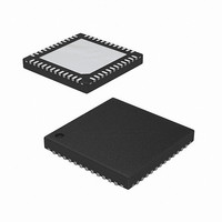
ISL6265AHRTZ Intersil, ISL6265AHRTZ Datasheet - Page 21

ISL6265AHRTZ
Manufacturer Part Number
ISL6265AHRTZ
Description
IC CTRLR MULTI-OUTPUT 48-TQFN
Manufacturer
Intersil
Datasheet
1.ISL6265AHRTZ.pdf
(23 pages)
Specifications of ISL6265AHRTZ
Applications
Controller, AMD SVI Capable Mobile
Voltage - Input
5 ~ 24 V
Number Of Outputs
3
Voltage - Output
0.5 ~ 1.55 V
Operating Temperature
-10°C ~ 100°C
Mounting Type
Surface Mount
Package / Case
48-TQFN
Lead Free Status / RoHS Status
Lead free / RoHS Compliant
Available stocks
Company
Part Number
Manufacturer
Quantity
Price
Company:
Part Number:
ISL6265AHRTZ
Manufacturer:
Intersil
Quantity:
800
Company:
Part Number:
ISL6265AHRTZ
Manufacturer:
INTERSIL
Quantity:
1 000
Part Number:
ISL6265AHRTZ
Manufacturer:
INTERSIL
Quantity:
20 000
Company:
Part Number:
ISL6265AHRTZ-T
Manufacturer:
HONEYWELL
Quantity:
100
Part Number:
ISL6265AHRTZ-T
Manufacturer:
INTERSIL
Quantity:
20 000
MOSFET Selection and Considerations
The choice of MOSFETs depends on the current each
MOSFET will be required to conduct, the switching
frequency, the capability of the MOSFETs to dissipate heat,
and the availability and nature of heat sinking and air flow.
Typically, a MOSFET cannot tolerate even brief excursions
beyond their maximum drain to source voltage rating. The
MOSFETs used in the power stage of the converter should
have a maximum V
upper voltage tolerance of the input power source and the
voltage spike that occurs when the MOSFETs switch.
There are several power MOSFETs readily available that are
optimized for DC/DC converter applications. The preferred
high-side MOSFET emphasizes low gate charge so that the
device spends the least amount of time dissipating power in the
linear region. The preferred low-side MOSFET emphasizes low
r
For the low-side (LS) MOSFET, the power loss can be
assumed to be conductive only and is written as Equation 24:
For the high-side (HS) MOSFET, the its conduction loss is
written as Equation 25:
For the high-side MOSFET, the switching loss is written as
Equation 26:
Where:
P
P
P
DS(ON)
CON_LS
CON_HS
SW_HS
FIGURE 12. NORMALIZED RMS INPUT CURRENT FOR
- I
- I
inductor current minus 1/2 of the inductor ripple current
current plus 1/2 of the inductor ripple current
VALLEY
PEAK
when fully saturated to minimize conduction loss.
0.3
0.2
0.1
0
=
≈
0
=
is the sum of the DC component of the inductor
I
V
---------------------------------------------------------------- -
LOAD
is the difference of the DC component of the
I
IN
LOAD
I
2-PHASE CONVERTER
P-P,N
•
I
VALLEY
2
= 0.75
2
0.2
r ⋅
DS
•
DS ON
r
DS ON
2
rating that exceeds the sum of the
(
DUTY CYCLE (V
(
•
t
ON
)_LS
0.4
)_HS
21
•
f
SW
•
(
•
1 D
D
+
–
V
------------------------------------------------------------ -
I
P-P,N
0.6
IN/
IN
)
I
V
•
P-P,N
O
I
= 0
PEAK
)
= 0.5
2
0.8
•
t
OFF
•
(EQ. 26)
(EQ. 24)
(EQ. 25)
f
SW
1.0
ISL6265A
Selecting The Bootstrap Capacitor
All three integrated drivers feature an internal bootstrap
schottky diode. Simply adding an external capacitor across
the BOOT and PHASE pins completes the bootstrap circuit.
The bootstrap function is also designed to prevent the
bootstrap capacitor from overcharging due to the large
negative swing at the PHASE node. This reduces voltage
stress on the BOOT and PHASE pins.
The bootstrap capacitor must have a maximum voltage
rating above PVCC + 4V and its capacitance value is
selected per Equation 27:
Where:
As an example, suppose the high-side MOSFET has a total
gate charge Q
200mV. The calculated bootstrap capacitance is 0.125µF; for
a comfortable margin, select a capacitor that is double the
calculated capacitance. In this example, 0.22µF will suffice.
Use a low temperature-coefficient ceramic capacitor.
PCB Layout Considerations
Power and Signal Layers Placement on the PCB
As a general rule, power layers should be close together,
either on the top or bottom of the board, with the weak analog
or logic signal layers on the opposite side of the board. The
ground-plane layer should be adjacent to the signal layer to
provide shielding. The ground plane layer should have an
island located under the IC, the compensation components,
and the FSET components. The island should be connected
to the rest of the ground plane layer at one point.
Component Placement
There are two sets of critical components in a DC/DC
converter; the power components and the small signal
components. The power components are the most critical
because they switch large amount of energy. The small
signal components connect to sensitive nodes or supply
critical bypassing current and signal coupling.
The power components should be placed first and these
include MOSFETs, input and output capacitors, and the
inductor. It is important to have a symmetrical layout for each
power train, preferably with the controller located equidistant
from each power train. Symmetrical layout allows heat to be
dissipated equally across all power trains. Keeping the
C
- t
- t
BOOT
- Q
- ΔV
saturation
high-side MOSFET
the boot capacitor each time the high-side MOSFET is
switched on
ON
OFF
g
BOOT
is the total gate charge required to turn on the
≥
is the time required to drive the device into
is the time required to drive the device into cut-off
----------------------- -
ΔV
, is the maximum allowed voltage decay across
Q
BOOT
g
g
, of 25nC at V
GS
= 5V, and a ΔV
BOOT
May 11, 2009
(EQ. 27)
of
FN6884.0


