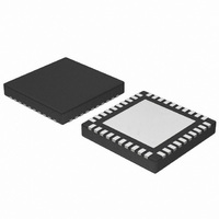
NCP4200MNR2G ON Semiconductor, NCP4200MNR2G Datasheet - Page 16

NCP4200MNR2G
Manufacturer Part Number
NCP4200MNR2G
Description
IC CONV SYNC BUCK PMBUS 40QFN
Manufacturer
ON Semiconductor
Datasheet
1.NCP4200MNR2G.pdf
(32 pages)
Specifications of NCP4200MNR2G
Applications
Converter, Intel VR11, VR11.1
Voltage - Input
1.7 ~ 24 V
Number Of Outputs
1
Voltage - Output
0.375 ~ 1.8 V
Operating Temperature
0°C ~ 85°C
Mounting Type
Surface Mount
Package / Case
40-VFQFN Exposed Pad
Output Voltage
0.375 V to 1.6 V
Output Current
500 uA
Input Voltage
1.7 V to 24 V
Switching Frequency
0.25 MHz to 6 MHz
Operating Temperature Range
0 C to + 85 C
Mounting Style
SMD/SMT
Duty Cycle (max)
100 %
Isolated/non-isolated
Non Isolated
Lead Free Status / RoHS Status
Lead free / RoHS Compliant
Available stocks
Company
Part Number
Manufacturer
Quantity
Price
Company:
Part Number:
NCP4200MNR2G
Manufacturer:
PHILIPS
Quantity:
124
delay time (TD5). Prior to the SS voltage reaching the
programmed VID DAC voltage and the PWRGD masking
time finishing, the PWRGD pin is held low. Once the SS
circuit reaches the programmed DAC voltage, the internal
timer operates.
and −500 mV. However these values can be adjusted over the
I
of Command Code 0xE0 and the low limit is programmed
using Bits <2:0> of Command code 0xE1. The following is
a table of the programmable values.
Power State Indicator
state of the load. If this input is pulled low, the load is in a low
power state and the controller asserts the ODN pin low,
which can be used to disable phases and maintain better
efficiency at lighter loads.
maintained to minimize output deviations as well as
providing full power load transients immediately after
exiting a low power state.
PSI is asserted. By default only phase 1 is enabled. The
number of phases enabled can be changed over the I
Interface. However extreme care should be taken to ensure
that OD1 is connected to all phases enabled during PSI. The
number of phases enabled during PSI is programmed using
Bits 6 and 7 of the MFR Config Command (0xD1).
2
Table 7. PWRGD High Limits
Table 8. PWRGD Low Limits
Table 9. # Phases Enabled During PSI
C Interface. The high limit is programmed using Bits <1:0>
The PWRGD circuitry also incorporates an initial turn−on
The default range for the PWRGD comparator is +300 mV
The PSI pin is an input used to determine the operating
The sequencing into and out of low power operation is
The user can program how many phases are enabled when
Code
Code
Code
000
001
010
100
101
011
110
111
00
01
10
11
00
01
10
11
PWRGD High Limits
PWRGD High Limits
PWRGD Low Limits
1−Phase (default)
+300mV (default)
−500mV (default)
2−Phases
+250 mV
+200 mV
+150 mV
−450 mV
−400 mV
−350 mV
−300 mV
−250 mV
−200 mV
−150 mV
1−Phase
1−Phase
http://onsemi.com
2
C
16
phases are enabled for normal operation. For example if 4
phases are enabled normally and 2 during PSI, then Phase 1
and Phase 3 will be enabled during PSI.
Output Crowbar
components of the supply, the PWM outputs are driven low
(turning on the low−side MOSFETs) when the output
voltage exceeds the upper crowbar threshold. This crowbar
action stops once the output voltage falls below the release
threshold of approximately 300 mV. The value for the
crowbar limit follows the programmable PWRGD high
limit.
as the reverse current builds up in the inductors. If the output
overvoltage is due to a short in the high−side MOSFET, this
action current limits the input supply, or blows its fuse
protecting the microprocessor from being destroyed.
Output Enable and UVLO
current to the controller must be higher than the UVLO
threshold and the EN pin must be higher than its 0.8 V
threshold. This initiates a system startup sequence. If either
UVLO or EN is less than their respective thresholds, the
NCP4200 is disabled. This holds the PWM outputs at
ground and forces PWRGD, ODN and OD1 signals low.
should be connected to the OD inputs of the external drivers
for the phases that are always on. The ODN pin should be
connected to the OD inputs of the external drivers on the
phases that are shut down during low power operation.
that both DRVH and DRVL are grounded. This feature is
important in preventing the discharge of the output
capacitors when the controller is shut off. If the driver
outputs are not disabled, a negative voltage can be generated
during output due to the high current discharge of the output
capacitors through the inductors.
Voltage Monitoring
reports this back in a register. The ADC range for the voltage
measurements is 0 V to 2.0 V. Voltages greater than 2.0 V can
be monitored using a resistor divider network. Voltage
measurements are 10 bits wide.
Shunt Resistor
12 V supply range. A trade−off can be made between the
power dissipated in the shunt resistor and the UVLO
threshold.
realize certain UVLO voltages. It also gives the maximum
power dissipated in the shunt resistor for these UVLO
voltages.
The actual phases enabled, depends upon how many
As part of the protection for the load and output
Turning on the low−side MOSFETs pulls down the output
For the NCP4200 to begin switching the input, supply
In the application circuit (see Figure 2), the OD1 pin
Grounding the driver OD inputs disables the drivers such
The NCP4200 can monitor the voltage on the EN pin and
The NCP4200 uses a shunt to generate 5.0 V from the
Figure 10 shows the typical resistor value needed to


