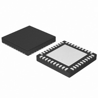
NCP4200MNR2G ON Semiconductor, NCP4200MNR2G Datasheet - Page 4

NCP4200MNR2G
Manufacturer Part Number
NCP4200MNR2G
Description
IC CONV SYNC BUCK PMBUS 40QFN
Manufacturer
ON Semiconductor
Datasheet
1.NCP4200MNR2G.pdf
(32 pages)
Specifications of NCP4200MNR2G
Applications
Converter, Intel VR11, VR11.1
Voltage - Input
1.7 ~ 24 V
Number Of Outputs
1
Voltage - Output
0.375 ~ 1.8 V
Operating Temperature
0°C ~ 85°C
Mounting Type
Surface Mount
Package / Case
40-VFQFN Exposed Pad
Output Voltage
0.375 V to 1.6 V
Output Current
500 uA
Input Voltage
1.7 V to 24 V
Switching Frequency
0.25 MHz to 6 MHz
Operating Temperature Range
0 C to + 85 C
Mounting Style
SMD/SMT
Duty Cycle (max)
100 %
Isolated/non-isolated
Non Isolated
Lead Free Status / RoHS Status
Lead free / RoHS Compliant
Available stocks
Company
Part Number
Manufacturer
Quantity
Price
Company:
Part Number:
NCP4200MNR2G
Manufacturer:
PHILIPS
Quantity:
124
Stresses exceeding Maximum Ratings may damage the device. Maximum Ratings are stress ratings only. Functional operation above the
Recommended Operating Conditions is not implied. Extended exposure to stresses above the Recommended Operating Conditions may affect
device reliability.
1. Refer to Electrical Characteristics and Application Information for Safe Operating Area.
2. This device series incorporates ESD protection and is tested by the following methods:
3. For information, please refer to our Soldering and Mounting Techniques Reference Manual, SOLDERRM/D.
4. Values based on copper area of 645 mm
5. Minimum V
ABSOLUTE MAXIMUM RATINGS
THERMAL CHARACTERISTICS
OPERATING RANGES
Input Voltage Range (Note 1)
FBRTN
PWM2 to PWM4, RAMPADJ
SW1 to SW4
SW1 to SW4 (< 200 ns)
All Other Inputs and Outputs
Storage Temperature Range
Operating Ambient Temperature Range
ESD Capability, Human Body Model (Note 2)
ESD Capability, Machine Body Model (Note 2)
Lead Temperature Soldering
Thermal Characteristics; QFN, 6mm x 6mm (Note 1)
Input Voltage (Note 5)
Output Voltage (Adjustable Version Only)
Ambient Temperature
ESD Human Body Model tested per AEC−Q100−002 (EIA/JESD22−A114)
ESD Machine Model tested per AEC−Q100−003 (EIA/JESD22−A115)
Latchup Current Maximum Rating: ≤150 mA per JEDEC standard: JESD78
Re−flow (SMD Styles Only, Pb−Free Versions (Note 3)
Thermal Resistance, Junction−to−Air (Note 4)
IN
= 1.7 V or (V
(Note 1)
Parameter
Parameter
Parameter
OUT
+ V
DO
), whichever is higher. Maximum Limit for V
2
(or 1 in
2
) of 1 oz copper thickness and FR4 PCB substrate.
http://onsemi.com
4
ESD
Symbol
Symbol
Symbol
V
ESD
V
T
T
R
FBRTN
V
V
STG
OUT
T
SLD
qJA
IN
IN
A
HBM
MM
OUT
= V
OUT(NOM)
0.375
Min
1.7
0
−0.3 to V
−0.3 to V
−65 to +150
−0.3 to 6.0
−0.3 to 0.3
−10 to +25
−10 to 100
−5 to +25
– 10%.
Value
Value
100
260
27
2
IN
IN
+ 0.3
+0.3
Max
1.8
24
85
°C/W
Unit
Unit
Unit
°C
°C
kV
°C
°C
V
V
V
V
V
V
V
V
V


