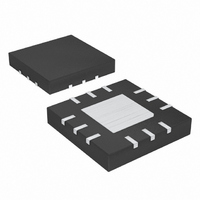
MAX1932ETC+T Maxim Integrated Products, MAX1932ETC+T Datasheet - Page 2

MAX1932ETC+T
Manufacturer Part Number
MAX1932ETC+T
Description
IC SUPPLY BIAS APD 12-TQFN
Manufacturer
Maxim Integrated Products
Datasheet
1.MAX1932ETC.pdf
(16 pages)
Specifications of MAX1932ETC+T
Applications
Controller, Fiber Optic Network
Voltage - Input
2.7 ~ 5.5 V
Number Of Outputs
1
Voltage - Output
4.5 ~ 90 V
Operating Temperature
0°C ~ 85°C
Mounting Type
Surface Mount
Package / Case
12-TQFN Exposed Pad
Lead Free Status / RoHS Status
Lead free / RoHS Compliant
ABSOLUTE MAXIMUM RATINGS
VIN to GND...............................................................-0.3V to +6V
DIN, SCLK, CS, FB to GND ......................................-0.3V to +6V
COMP, DACOUT, GATE, CL to GND ...........-0.3V to (V
CS+, CS- to GND .................................................-0.3V to +110V
Continuous Power Dissipation (T
Digitally Controlled, 0.5% Accurate,
Safest APD Bias Supply
Stresses beyond those listed under “Absolute Maximum Ratings” may cause permanent damage to the device. These are stress ratings only, and functional
operation of the device at these or any other conditions beyond those indicated in the operational sections of the specifications is not implied. Exposure to
absolute maximum rating conditions for extended periods may affect device reliability.
ELECTRICAL CHARACTERISTICS
(V
2
GENERAL
Input Supply Range
V
Operating Supply Current
V
Input Resistance for CS+/CS-
Current-Limit Threshold
for CS+/CS-
Common-Mode Rejection
of Current Threshold
Gate-Driver Resistance
FB Input Bias Current
FB Voltage
FB Voltage
Temperature Coefficient
FB to COMP Transconductance
COMP Pulldown Resistance
in Shutdown
D AC OU T to FB V ol tag e D i ffer ence
D AC OU T Differential Nonlinearity
(Note 1)
D AC OU T Voltage Temperature
Coefficient
DACOUT Load Regulation
Switching Frequency
GATE Maximum On-Time
IN
12-Pin Thin QFN (derate 16.9mW/°C above +70°C) .1349mW
IN
IN
_______________________________________________________________________________________
= 3.3V, CS = SCLK = D
Undervoltage Lockout
Shutdown Supply Current
PARAMETER
IN
= 3.3V, CS+ = CS- = 45V, Circuit of Figure 2, T
A
= +70°C)
TCV
SYMBOL
TCV
I
UVLO
SHDN
f
V
DACOUT
t
V
OSC
I
ON
IN
FB
IN
FB
Both rise/fall, hysteresis = 100mV
00 hex loaded to DAC
Resistance from either pin to ground
CS+ = 3V to 100V
Gate high or low, I
T
T
COMP = 1.5V
DAC code = 00 hex
DAC code = FF hex
DAC Code = 01 to FF hex,
DAC guaranteed monotonic
DAC code = 0F to FF hex, source or sink
50µA
A
A
= +25°C
= 0°C to +85°C
IN
+0.3V)
CONDITIONS
GATE
Operating Temperature Range ...........................-40°C to +85°C
Junction Temperature ......................................................+150°C
Storage Temperature Range .............................-65°C to +150°C
Lead Temperature (soldering 10s) ..................................+300°C
= ±50mA
A
= 0°C to +85°C, unless otherwise noted.)
1.24375 1.2500 1.25625
1.24250 1.2500 1.25750
1.80
MIN
250
2.7
2.1
0.5
-25
50
-3
-1
-1
0.0007
0.0007
±0.005
TYP
2.00
110
300
0.5
25
1
5
3
MAX
2.20
+25
200
100
340
5.5
2.6
2.0
+3
+1
+1
65
10
1
UNITS
%/°C
%/°C
LSB
%/V
kHz
MΩ
mA
mV
mV
µA
nA
µS
µs
Ω
Ω
V
V
V
V


