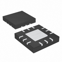
MAX1932ETC+T Maxim Integrated Products, MAX1932ETC+T Datasheet - Page 8

MAX1932ETC+T
Manufacturer Part Number
MAX1932ETC+T
Description
IC SUPPLY BIAS APD 12-TQFN
Manufacturer
Maxim Integrated Products
Datasheet
1.MAX1932ETC.pdf
(16 pages)
Specifications of MAX1932ETC+T
Applications
Controller, Fiber Optic Network
Voltage - Input
2.7 ~ 5.5 V
Number Of Outputs
1
Voltage - Output
4.5 ~ 90 V
Operating Temperature
0°C ~ 85°C
Mounting Type
Surface Mount
Package / Case
12-TQFN Exposed Pad
Lead Free Status / RoHS Status
Lead free / RoHS Compliant
(<10pF) are recommended to minimize losses. A small-
signal silicon switching diode is suitable if efficiency is
not critical.
The output capacitors of the MAX1932 must have high
enough voltage rating to operate with the V
required. Output capacitor effective series resistance
(ESR) determines the amplitude of the high-frequency
ripple seen on the output voltage. In the typical applica-
tion circuit, a second RC formed by R1 and C3 further
reduces ripple.
The input bypass capacitor reduces the peak currents
drawn from the voltage source and reduces noise
caused by the MAX1932’s switching action. The input
source impedance determines the size of the capacitor
required at the input (VIN). A low ESR capacitor is rec-
ommended. A 1µF ceramic capacitor is adequate for
most applications. Place the bypass capacitor as close
as possible to the VIN and GND pins.
Current limit is used to set the maximum delivered out-
put current. In the typical application circuit, MAX1932
is designed to current limit at:
Note that I
back divider (if sensing feedback after R1) and the
input current of CS-.
Compensation components, R7 and C4, introduce a
pole and a zero necessary to stabilize the MAX1932
(see Figure 6). The dominant pole, POLE1, is formed by
the output impedance of the error amplifier (R
C4. The R7/C4 zero, ZERO1, is selected to cancel the
pole formed by the output filter cap C3 and output load
R
should be at least a decade past the crossover fre-
quency to not affect stability:
POLE1 (dominant pole) = 1 / (2π
ZERO1 (integrator zero) = 1 / (2π
POLE2 (output load pole) = K1 / (2π
POLE3 (output filter pole) = 1 / (2π
The DC open-loop gain is given by:
Digitally Controlled, 0.5% Accurate,
Safest APD Bias Supply
8
LD
_______________________________________________________________________________________
, POLE2. The additional pole of R1/C3, POLE3,
LIMIT
Input Bypass Capacitor Selection
Current-Sense Resistor Selection
Output Filter Capacitor Selection
must include current drawn by the feed-
A
OL
Stability and Compensation
= K2
R
1
=
✕
I
LIMIT
Component Selection
2
Gm
V
✕
✕
✕
R
✕
R
R7
EA
✕
EA
R1
R
✕
✕
LD
✕
C4)
C4)
C3)
✕
(C2 + C3))
EA
) and
OUT
where R
g
R
and the load resistance.
A properly compensated MAX1932 results in a gain vs.
frequency plot that crosses 0dB with a single pole
slope (20dB per decade). See Figure 6.
Table 1 lists suggested component values for several
typical applications.
The current-limit sense resistor is typically used as part
of an output lowpass filter to reduce noise and ripple.
For further reduction of noise, an LC filter can be added
as shown in Figure 7. Output ripple and noise with and
without the LC filter are shown in the Typical Operating
Characteristics. If a post LC filter is used, it is best to
use a coil with fairly large resistance (or a series resis-
tor) so that ringing at the response peak of the LC filter
is damped. For a 330µH and 1µF filter, 22Ω accom-
plishes this, but a resistor is not needed if the coil resis-
tance is greater than 15Ω.
The MAX1932 features 0.5% feedback accuracy. The
total voltage accuracy of a complete APD bias circuit is
the sum of the FB set-point accuracy, plus resistor ratio
error and temperature coefficient. If absolute accuracy
is critical, the best resistor choice is an integrated net-
work with specified ratio tolerance and temperature
coefficient. If using discrete resistors in high-accuracy
applications, pay close attention to resistor tolerance
and temperature coefficients.
APDs exhibit a change in gain as a function of tempera-
ture. This gain change can be compensated with an
appropriate adjustment in bias voltage. For this reason
it may be desirable to vary the MAX1932 output voltage
as a function of temperature. This can be done in soft-
K
K
⎛
⎜
⎜
⎝
M
LD
1
2
=
⎛
⎜
⎝
= 110µS,
=
V
is the parallel combination of feedback network
2
0 75
OUT
V
×
V
V
.
FB
OUT
EA
V
OUT
OUT
(
(
-
Volts
= 310MΩ,
Volts
V
-
IN
V
-
IN
Output Accuracy and Feedback
⎞
⎟
⎠
V
)
IN
)
R
×
2
LD
×
2
Temperature Compensation
L Henries
×
×
(
V
T
2
OUT
(
Further Noise Reduction
×
sec
V
IN
ond
-
V
IN
)
)
Resistor Selection
⎞
⎟
⎟
⎠
×


