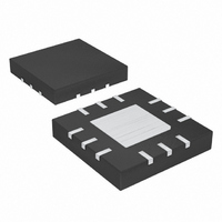
MAX1932ETC+T Maxim Integrated Products, MAX1932ETC+T Datasheet - Page 6

MAX1932ETC+T
Manufacturer Part Number
MAX1932ETC+T
Description
IC SUPPLY BIAS APD 12-TQFN
Manufacturer
Maxim Integrated Products
Datasheet
1.MAX1932ETC.pdf
(16 pages)
Specifications of MAX1932ETC+T
Applications
Controller, Fiber Optic Network
Voltage - Input
2.7 ~ 5.5 V
Number Of Outputs
1
Voltage - Output
4.5 ~ 90 V
Operating Temperature
0°C ~ 85°C
Mounting Type
Surface Mount
Package / Case
12-TQFN Exposed Pad
Lead Free Status / RoHS Status
Lead free / RoHS Compliant
The MAX1932 uses a constant frequency, PWM, con-
troller architecture. This controller sets the switch on-
time and drives an external N-channel MOSFET (see
Figure 1). As the load varies, the error amplifier sets the
inductor peak current necessary to supply the load and
regulate the output voltage.
The MAX1932 uses an external resistor at CS+ and CS-
to sense the output current (see Figure 2). The typical
current-limit threshold is 2V. CL is designed to help find
the optimum APD bias point by going low to indicate
when the APD reaches avalanche and that current limit
has been activated. To minimize noise, CL only
changes state on an internal oscillator edge.
An internal digital-to-analog converter can be used to
control the output voltage of the DC-DC converter
(Figure 2). The DAC output is changed through an SPI™
serial interface using an 8-bit control byte. On power-up,
the DAC defaults to FF hex (1.25V), which corresponds
to a minimum boost converter output voltage.
Alternately, the output voltage can be set with external
resistors, an external DAC, or a voltage source. Output
span and offset are independently settable with exter-
Digitally Controlled, 0.5% Accurate,
Safest APD Bias Supply
SPI is a trademark of Motorola, Inc.
6
PIN
_______________________________________________________________________________________
10
11
12
1
2
3
4
5
6
7
8
9
DACOUT
NAME
COMP
SCLK
GATE
GND
CS+
DIN
CS-
VIN
CL
FB
CS
DAC Serial Clock Input
DAC Serial Data Input
Current-Limit Indicator Flag. CL = 0 indicates that the part is in current limit. Logic high level = VIN.
Current-Limit Plus Sense Input. Connect a resistor from CS+ to CS- in series with the output. The differential
threshold is 2V. CS+ has typically 1MΩ resistance to ground.
Current-Limit Minus Sense Input. CS- has typically 1MΩ resistance to ground.
Internal DAC Output. Generates a control voltage for adjustable output operation. DACOUT can source or
sink 50µA.
Feedback input. Connect to a resistive voltage-divider between the output voltage (V
output voltage. The feedback set point is 1.25V.
Compensation Pin. Compensates the DC-DC converter control loop with a series RC to GND. COMP is
actively discharged to ground during shutdown or undervoltage conditions.
Ground
Gate-Driver Output for External N-FET
IC Supply Voltage (2.7V to 5.5V). Bypass VIN with a 1µF or greater ceramic capacitor.
DAC Chip-Select Input
Detailed Description
Fixed Frequency PWM
Output Current Limit
Output Control DAC
nal resistors. See the Applications Information section
for output control equations.
Use an SPI-compatible 3-wire serial interface with the
MAX1932 to control the DAC output voltage and to shut
down the MAX1932. Figures 4 and 5 show timing diagrams
for the SPI protocol. The MAX1932 is a write-only device
and uses CS along with SCLK and DIN to communicate.
The serial port is always operational when the device is
powered. To shut down the DC-DC converter portion only,
update the DAC registers to 00 hex.
Feedback can be taken from in front of, or after, the cur-
rent-limit sense resistor. The current-limit sense resistor
forms a lowpass filter with the output capacitor. Taking
feedback after the current-limit sense resistor (see Figure
2), optimizes the output voltage accuracy, but requires
overcompensation, which slows down the control loop
response. For faster response, the feedback can be
taken from in front of the current-sense resistor (see
Figure 3). This configuration however, makes the output
voltage more sensitive to load variation and degrades
output accuracy by an amount equal to the load current
times the current-sense resistor value.
FUNCTION
Applications Information
Voltage Feedback Sense Point
SPI Interface/Shutdown
Pin Description
OUT
) and FB to set the


