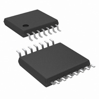
LM25010MH/NOPB National Semiconductor, LM25010MH/NOPB Datasheet - Page 11

LM25010MH/NOPB
Manufacturer Part Number
LM25010MH/NOPB
Description
IC BUCK ADJ 1A 14TSSOP
Manufacturer
National Semiconductor
Type
Step-Down (Buck)r
Specifications of LM25010MH/NOPB
Internal Switch(s)
Yes
Synchronous Rectifier
No
Number Of Outputs
1
Voltage - Output
2.5 ~ 37 V
Current - Output
1A
Frequency - Switching
100kHz ~ 1MHz
Voltage - Input
6 ~ 42 V
Operating Temperature
-40°C ~ 125°C
Mounting Type
Surface Mount
Package / Case
14-TSSOP Exposed Pad, 14-eTSSOP 14-HTSSOP
Dc To Dc Converter Type
Step Down
Pin Count
14
Input Voltage
42V
Output Voltage
2.5 to 37V
Switching Freq
100 to 1000KHz
Output Current
1A
Efficiency
95%
Package Type
TSSOP EP
Output Type
Adjustable
Switching Regulator
Yes
Mounting
Surface Mount
Input Voltage (min)
6V
Operating Temperature Classification
Automotive
Current, Input Bias
1 nA
Current, Output
1 A
Current, Supply
645 μA
Frequency, Oscillator
1 MHz
Regulator Type
Buck (Step-Down), Switching
Resistance, Thermal, Junction To Case
5.2 °C/W
Temperature, Operating, Range
-40 to +125 °C
Voltage, Input
6 to 42 V
Voltage, Output
7 V
For Use With
LM25010EVAL - BOARD EVALUATION LM25010
Lead Free Status / RoHS Status
Lead free / RoHS Compliant
Power - Output
-
Lead Free Status / Rohs Status
Compliant
Other names
*LM25010MH
*LM25010MH/NOPB
LM25010MH
*LM25010MH/NOPB
LM25010MH
Available stocks
Company
Part Number
Manufacturer
Quantity
Price
N - Channel Buck Switch and Driver
The LM25010 integrates an N-Channel buck switch and as-
sociated floating high voltage gate driver. The peak current
through the buck switch should not exceed 2A, and the load
current should not exceed 1.5A. The gate driver circuit is
powered by the external bootstrap capacitor between BST
and SW (C4), which is recharged each off-time from V
through the internal high voltage diode. The minimum off-
time, nominally 260 ns, ensures sufficient time during each
cycle to recharge the bootstrap capacitor. A 0.022 µF ceramic
capacitor is recommended for C4.
Soft-Start
The soft-start feature allows the regulator to gradually reach
a steady state operating point, thereby reducing startup
stresses and current surges. At turn-on, while V
the under-voltage threshold (t1 in Figure 1), the SS pin is in-
ternally grounded, and V
the under-voltage threshold (UVLO) an internal 11.5 µA cur-
rent source charges the external capacitor (C6) at the SS pin
to 2.5V (t2 in Figure 1). The increasing SS voltage at the non-
inverting input of the regulation comparator gradually increas-
es the output voltage from zero to the desired value. The soft-
start feature keeps the load inductor current from reaching the
current limit threshold during start-up, thereby reducing inrush
currents.
An internal switch grounds the SS pin if V
der-voltage lock-out threshold, or if the circuit is shutdown
using the RON/SD pin.
Thermal Shutdown
The LM25010 should be operated below the Maximum Op-
erating Junction Temperature rating. If the junction tempera-
ture increases during a fault or abnormal operating condition,
the internal Thermal Shutdown circuit activates typically at
175°C. The Thermal Shutdown circuit reduces power dissi-
pation by disabling the buck switch and the on-timer. This
feature helps prevent catastrophic failures from accidental
device overheating. When the junction temperature reduces
below approximately 155°C (20°C typical hysteresis), normal
operation resumes.
OUT
is held at 0V. When V
FIGURE 4. Inductor Current - Current Limit Operation
CC
is below the un-
CC
CC
is below
exceeds
CC
11
Applications Information
EXTERNAL COMPONENTS
The procedure for calculating the external components is il-
lustrated with a design example. Referring to the Block Dia-
gram, the circuit is to be configured for the following
specifications:
•
•
•
•
•
•
R1 and R2: These resistors set the output voltage, and their
ratio is calculated from:
R1/R2 calculates to 1.0. The resistors should be chosen from
standard value resistors in the range of 1.0 kΩ - 10 kΩ. A value
of 1.0 kΩ will be used for R1 and for R2.
R
inal frequency, or from Equation 6 if the on-time at a particular
V
er inductor and capacitors (value, size and cost), but higher
switching losses. A lower frequency means a higher efficien-
cy, but with larger components. Generally, if PC board space
is tight, a higher frequency is better. The resulting on-time and
frequency have a ±25% tolerance. Using equation 7 at a
nominal V
A value of 200 kΩ will be used for R
frequency of 161 kHz at V
L1: The guideline for choosing the inductor value in this ex-
ample is that it must keep the circuit’s operation in continuous
conduction mode at minimum load current. This is not a strict
requirement since the LM25010 regulates correctly when in
discontinuous conduction mode, although at a lower frequen-
cy. However, to provide an initial value for L1 the above
guideline will be used.
IN
ON
V
V
F
Minimum load current = 200 mA
Maximum load current = 1.0A
Softstart time = 5 ms.
is important. A higher frequency generally means a small-
, F
S
OUT
IN
= 175 kHz
S
= 6V to 40V
: R
= 5V
IN
ON
of 8V,
can be chosen using Equation 7 to set the nom-
R1/R2 = (V
IN
OUT
= 6V, and 203 kHz at V
/2.5V) - 1
ON
, yielding a nominal
20172720
www.national.com
IN
= 40V.
(10)


