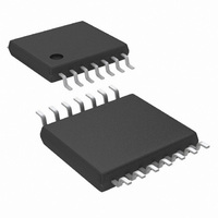
LM25010MH/NOPB National Semiconductor, LM25010MH/NOPB Datasheet - Page 3

LM25010MH/NOPB
Manufacturer Part Number
LM25010MH/NOPB
Description
IC BUCK ADJ 1A 14TSSOP
Manufacturer
National Semiconductor
Type
Step-Down (Buck)r
Specifications of LM25010MH/NOPB
Internal Switch(s)
Yes
Synchronous Rectifier
No
Number Of Outputs
1
Voltage - Output
2.5 ~ 37 V
Current - Output
1A
Frequency - Switching
100kHz ~ 1MHz
Voltage - Input
6 ~ 42 V
Operating Temperature
-40°C ~ 125°C
Mounting Type
Surface Mount
Package / Case
14-TSSOP Exposed Pad, 14-eTSSOP 14-HTSSOP
Dc To Dc Converter Type
Step Down
Pin Count
14
Input Voltage
42V
Output Voltage
2.5 to 37V
Switching Freq
100 to 1000KHz
Output Current
1A
Efficiency
95%
Package Type
TSSOP EP
Output Type
Adjustable
Switching Regulator
Yes
Mounting
Surface Mount
Input Voltage (min)
6V
Operating Temperature Classification
Automotive
Current, Input Bias
1 nA
Current, Output
1 A
Current, Supply
645 μA
Frequency, Oscillator
1 MHz
Regulator Type
Buck (Step-Down), Switching
Resistance, Thermal, Junction To Case
5.2 °C/W
Temperature, Operating, Range
-40 to +125 °C
Voltage, Input
6 to 42 V
Voltage, Output
7 V
For Use With
LM25010EVAL - BOARD EVALUATION LM25010
Lead Free Status / RoHS Status
Lead free / RoHS Compliant
Power - Output
-
Lead Free Status / Rohs Status
Compliant
Other names
*LM25010MH
*LM25010MH/NOPB
LM25010MH
*LM25010MH/NOPB
LM25010MH
Available stocks
Company
Part Number
Manufacturer
Quantity
Price
Pin Descriptions
LLP-10
10
1
2
3
4
5
6
7
8
9
Pin Number
TSSOP-14
1,7,8,14
10
11
12
13
2
3
4
5
6
9
RON/SD
SGND
Name
ISEN
RTN
VCC
BST
VIN
SW
NC
FB
SS
EP
Switching Node
Boost pin for bootstrap capacitor
Current sense
Current Sense Ground
Circuit Ground
Voltage feedback input from the
regulated output
Softstart
On-time control and shutdown
Output of the bias regulator
Input supply voltage
No connection.
Exposed Pad
Description
3
Internally connected to the buck switch source.
Connect to the inductor, free-wheeling diode, and
bootstrap capacitor.
Connect a capacitor from SW to the BST pin. The
capacitor is charged from VCC via an internal diode
during the buck switch off-time.
During the buck switch off-time, the inductor current
flows through the internal sense resistor, and out of
the ISEN pin to the free-wheeling diode. The current
limit comparator keeps the buck switch off if the ISEN
current exceeds 1.25A (typical).
Re-circulating current flows into this pin to the current
sense resistor.
Ground return for all internal circuitry other than the
current sense resistor.
Input to both the regulation and over-voltage
comparators. The FB pin regulation level is 2.5V.
An internal 11.5 µA current source charges the SS pin
capacitor to 2.5V to soft-start the reference input of
the regulation comparator.
An external resistor from VIN to the RON/SD pin sets
the buck switch on-time. Grounding this pin shuts
down the regulator.
The voltage at VCC is nominally equal to V
< 8.9V, and regulated at 7V for V
a 0.47 µF, or larger capacitor from VCC to ground, as
close as possible to the pins. An external voltage can
be applied to this pin to reduce internal dissipation if
V
VCC to VIN if V
Nominal input range is 6V to 42V. Input bypass
capacitors should be located as close as possible to
the VIN pin and RTN pins.
No internal connection. Can be connected to ground
plane to improve heat dissipation.
Exposed metal pad on the underside of the device. It
is recommended to connect this pad to the PC board
ground plane to aid in heat dissipation.
IN
is greater than 8.9V. MOSFET body diodes clamp
Application Information
CC
> V
IN
.
IN
> 8.9V. Connect
www.national.com
IN
for V
IN


