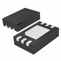
LTC3549EDCB#TRPBF Linear Technology, LTC3549EDCB#TRPBF Datasheet

LTC3549EDCB#TRPBF
Specifications of LTC3549EDCB#TRPBF
Available stocks
Related parts for LTC3549EDCB#TRPBF
LTC3549EDCB#TRPBF Summary of contents
Page 1
... LT, LTC and LTM are registered trademarks of Linear Technology Corporation. Burst Mode is a registered trademark of Linear Technology Corporation. All other trademarks are the property of their respective owners. Protected by U.S. Patents, including 5481178, 6580258, 6304066, 6127815, 6498466, 6611131. ...
Page 2
LTC3549 ABSOLUTE AXI U RATI GS (Note 1) Input Supply Voltage ................................... –0. RUN MODE Voltages .............–0. Voltage < 100ns Pulse .............–0. Operating Temperature Range (Note 2) ...
Page 3
ELECTRICAL CHARACTERISTICS temperature range, otherwise specifi cations are at T SYMBOL PARAMETER I Input DC Bias Current S Active Mode Sleep Mode Shutdown f Nominal Oscillator Frequency OSC t Soft-Start Period P-Channel FET PFET DS(ON) R ...
Page 4
LTC3549 W U TYPICAL PERFOR A CE CHARACTERISTICS (From Typical Application on the front page, except for the resistive divider resistor values) Effi ciency/Power Loss vs Load Current 1.5V, Burst Mode OUT 100 ...
Page 5
W U TYPICAL PERFOR A CE CHARACTERISTICS (From Typical Application on the front page, except for the resistive divider resistor values) Oscillator Frequency vs Temperature 2. 1.6V IN 2.25 2. 4.2V ...
Page 6
LTC3549 W U TYPICAL PERFOR A CE CHARACTERISTICS (From Typical Application on the front page, except for the resistive divider resistor values) Start-Up from Shutdown Burst Mode Operation V OUT 500mV/DIV V 1V/DIV RUN I L 50mA/DIV V = 3.6V ...
Page 7
CTIO S V (Pin 1): Main Supply Pin. Must be closely decoupled IN to GND, Pins 2 and 7, with a 4.7µF or greater ceramic capacitor. GND (Pin 2): N/C. Ground this pin. SW (Pin ...
Page 8
LTC3549 U OPERATIO Main Control Loop The LTC3549 uses a constant-frequency, current mode step-down architecture. Both the main (P-channel MOSFET) and synchronous (N-channel MOSFET) switches are internal. During normal operation, the internal top power MOSFET is turned on each cycle ...
Page 9
OPERATION be defi ned by the combination of the current needed to charge the output capacitance and the current provided to the load as the output voltage ramps up. The start- APPLICATIO S I FOR ATIO The basic ...
Page 10
LTC3549 U U APPLICATIO S I FOR ATIO tions do not offer much relief. Note that the capacitor manufacturer’s ripple current ratings are often based on 2000 hours of life. This makes it advisable to further derate the capacitor, or ...
Page 11
U U APPLICATIO S I FOR ATIO Effi ciency Considerations The effi ciency of a switching regulator is equal to the output power divided by the input power times 100 often useful to analyze individual losses to determine ...
Page 12
LTC3549 U U APPLICATIO S I FOR ATIO Thermal Considerations In most applications the LTC3549 does not dissipate much heat due to its high effi ciency. But, in applications where the LTC3549 is running at high ambient temperature with low ...
Page 13
U U APPLICATIO S I FOR ATIO Board Layout Considerations When laying out the printed circuit board, the following checklist should be used to ensure proper operation of the LTC3549. These items are also illustrated graphically in the layout diagram ...
Page 14
LTC3549 U U APPLICATIO S I FOR ATIO Design Example As a design example, assume the LTC3549 is used in a 2-alkaline cell battery-powered application. The V operating from a maximum of 3.1V down to about 1.8V. The load current ...
Page 15
... NOTE 6) 0.200 REF Information furnished by Linear Technology Corporation is believed to be accurate and reliable. However, no responsibility is assumed for its use. Linear Technology Corporation makes no representa- tion that the interconnection of its circuits as described herein will not infringe on existing patent rights. U DCB Package 6-Lead Plastic DFN (2mm × ...
Page 16
... Step-Down DC/DC Converter LTC3410/LTC3410B 300mA, 2.25MHz, Synchronous Step-Down DC/DC Converter LTC3411 1.25A (I ), 4MHz, Synchronous OUT Step-Down DC/DC Converter VLDO and ThinSOT are trademarks of Linear Technology Corporation. Linear Technology Corporation 16 1630 McCarthy Blvd., Milpitas, CA 95035-7417 (408) 432-1900 FAX: (408) 434-0507 ● L1, 4.7µH* IN ...


