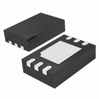
LTC3549EDCB#TRPBF Linear Technology, LTC3549EDCB#TRPBF Datasheet - Page 14

LTC3549EDCB#TRPBF
Manufacturer Part Number
LTC3549EDCB#TRPBF
Description
IC REG BUCK 250MA 6-DFN
Manufacturer
Linear Technology
Type
Step-Down (Buck)r
Datasheet
1.LTC3549EDCBTRMPBF.pdf
(16 pages)
Specifications of LTC3549EDCB#TRPBF
Internal Switch(s)
Yes
Synchronous Rectifier
Yes
Number Of Outputs
1
Voltage - Output
0.61 ~ 5.5 V
Current - Output
250mA
Frequency - Switching
2.25MHz
Voltage - Input
1.6 ~ 5.5 V
Operating Temperature
-40°C ~ 85°C
Mounting Type
Surface Mount
Package / Case
6-DFN
Lead Free Status / RoHS Status
Lead free / RoHS Compliant
Power - Output
-
Available stocks
Company
Part Number
Manufacturer
Quantity
Price
APPLICATIO S I FOR ATIO
LTC3549
Design Example
As a design example, assume the LTC3549 is used in a
2-alkaline cell battery-powered application. The V
operating from a maximum of 3.1V down to about 1.8V.
The load current requirement is a maximum of 250mA
but most of the time it will be in standby mode, requiring
only 2mA. Effi ciency at both low and high load currents
is important. Output voltage is 1.5V. With this information
we can calculate L using Equation 3:
14
L
=
f
V
Figure 4b. Burst Mode Effi ciency, V
•
OUT
∆
100
90
80
70
60
50
40
30
20
10
I
0
L
0.1
⎛
⎝ ⎜
1
–
U
V
V
V
OUT
IN
1
IN
V
LOAD CURRENT (mA)
= 1.8
IN
= 2.5
⎞
⎠ ⎟
U
10
1.8V TO
V
3.1V
IN
V
IN
= 3.1
*TDK VLF3012AT-3R3MR87
W
100
Figure 4a. High Effi ciency Step-Down Regulator
OUT
C
4.7µF
CERAMIC
IN
3549 F04b
1000
= 1.5V
U
IN
RUN
V
MODE
will be
IN
LTC3549
(3)
GND
V
SW
FB
Substituting V
f = 2.25MHz in Equation 3 gives:
For best effi ciency choose a 350mA or greater inductor
with less than 0.3Ω series resistance. C
RMS current rating of at least 0.125A ≅ I
temperature.
For the feedback resistors, choose R2 = 137k. Then, from
Equation 3, R1 is 200k. Figure 4 shows the complete circuit
along with its effi ciency curve.
L
R2
137k
3.3µH*
=
22pF
200k
CL
R1
L1
AC COUPLED
2 25
100mV/DIV
200mA/DIV
200mA/DIV
.
I
V
LOAD
OUT
MHz
I
L
OUT
V
V
I
Figure 4c. Load Step Response
LOAD
IN
OUT
1
= 2.5V
•
= 1.5V, V
= 1.5V
3549 F04a
C
4.7µF
CERAMIC
= 100mA to 250mA
100
OUT
V
1.5V
mA
OUT
20µs/DIV
1 5 1
IN
.
= 3.1V, ΔI
⎛
⎝ ⎜
–
1 5
3 1
.
.
L
IN
⎞
⎠ ⎟
3549 F04c
= 100mA and
LOAD(MAX)
≅
will require an
3 3
.
µ
H
/2 at
3549f


