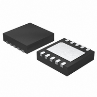
LTC3548EDD-1#TRPBF Linear Technology, LTC3548EDD-1#TRPBF Datasheet

LTC3548EDD-1#TRPBF
Specifications of LTC3548EDD-1#TRPBF
Available stocks
Related parts for LTC3548EDD-1#TRPBF
LTC3548EDD-1#TRPBF Summary of contents
Page 1
... The LTC3548-1 is available in both thin (0.75mm) and ultrathin (0.55mm) 3mm × 3mm DFN packages. L, LT, LTC, LTM, Linear Technology, the Linear logo and Burst Mode are registered trademarks of Linear Technology Corporation. All other trademarks are the property of their respective owners. Protected by U.S. Patents, including 5481178, 6127815, 6304066, 6498466, 6580258 6611131.. 2.2μ ...
Page 2
... TO A 4-LAYER BOARD) ORDER INFORMATION LEAD FREE FINISH TAPE AND REEL LTC3548EDD-1#PBF LTC3548EDD-1#TRPBF LTC3548EKD-1#PBF LTC3548EKD-1#TRPBF Consult LTC Marketing for parts specifi ed with wider operating temperature ranges. Consult LTC Marketing for information on non-standard lead based fi nish parts. For more information on lead free part marking, go to: http://www.linear.com/leadfree/ For more information on tape and reel specifi ...
Page 3
ELECTRICAL CHARACTERISTICS temperature range, otherwise specifi cations are at T SYMBOL PARAMETER V Operating Voltage Range IN V Output Voltage OUT1 V Output Voltage OUT2 ΔV Reference Voltage Line Regulation LINE REG ΔV Output Voltage Load Regulation LOAD REG I ...
Page 4
LTC3548-1 TYPICAL PERFORMANCE CHARACTERISTICS Effi ciency vs Input Voltage 100 100mA OUT 800mA I = 10mA OUT OUT 1mA OUT 2.5 4 4.5 3 3.5 ...
Page 5
TYPICAL PERFORMANCE CHARACTERISTICS Effi ciency vs Load Current 100 3. 2. 1.8V OUT1 65 NO LOAD ON OTHER CHANNEL CIRCUIT OF FIGURE 3 60 ...
Page 6
LTC3548-1 BLOCK DIAGRAM REGULATOR 0.6V EA – OUT1 FB1 – 0.55V R3 UVDET + + OVDET – 0.65V SHUTDOWN 8 RUN1 0.6V REF OSC 6 RUN2 REGULATOR 2 (IDENTICAL ...
Page 7
OPERATION The LTC3548-1 uses a constant-frequency, current mode architecture. The operating frequency is set at 2.25MHz. Both channels share the same clock and run in-phase. The output voltage is set by an internal divider. An error amplifi er compares the ...
Page 8
LTC3548-1 APPLICATIONS INFORMATION A general LTC3548-1 application circuit is shown in Figure 2. External component selection is driven by the load requirement, and begins with the selection of the inductor L. Once the inductor is chosen, C can be selected. ...
Page 9
APPLICATIONS INFORMATION where the maximum average output current I the peak current minus half the peak-to-peak ripple cur- rent – ΔI /2. MAX LIM L This formula has a maximum /2. This ...
Page 10
... I can be monitored OUT 1. The V Electrical Characteristics which excludes MOSFET driver and control currents. V (<0.1%) loss that increases with V Hot Swap is a trademark of Linear Technology Corporation. , causing a rapid drop in OUT quiescent current losses, 4) other losses. current is the DC supply current given in the ...
Page 11
APPLICATIONS INFORMATION 2. The switching current is the sum of the MOSFET driver and control currents. The MOSFET driver current re- sults from switching the gate capacitance of the power MOSFETs. Each time a MOSFET gate is switched from low ...
Page 12
LTC3548-1 APPLICATIONS INFORMATION Design Example As a design example, consider using the LTC3548 portable application with a Li-Ion battery. The battery provides 2.8V to 4.2V. The load requires a maximum IN of 800mA in active ...
Page 13
APPLICATIONS INFORMATION GND VIA TO V OUT1 GND Figure 4. LTC3548-1 Layout Diagram Effi ciency vs Load Current 100 1.8V OUT1 1.575V OUT2 ...
Page 14
LTC3548-1 PACKAGE DESCRIPTION 3.55 0.05 1.65 0.05 2.15 0.05 (2 SIDES) 0.25 0.05 RECOMMENDED SOLDER PAD PITCH AND DIMENSIONS PIN 1 TOP MARK (SEE NOTE 6) 0.200 REF 14 DD Package 10-Lead Plastic DFN (3mm × 3mm) (Reference LTC DWG ...
Page 15
... SHADED AREA IS ONLY A REFERENCE FOR PIN 1 LOCATION ON THE Information furnished by Linear Technology Corporation is believed to be accurate and reliable. However, no responsibility is assumed for its use. Linear Technology Corporation makes no representa- tion that the interconnection of its circuits as described herein will not infringe on existing patent rights. ...
Page 16
... V = 0.8V 26μA, IN OUT(MIN 2.5V to 5.5V 0.8V 60μA, IN OUT(MIN 2.5V to 5.5V 0.8V 60μA, IN OUT(MIN 2.25V to 5.5V 0.8V 64μA, IN OUT(MIN 2.5V to 5.5V 2.5V 25μA, IN OUT(MIN 2.5V to 5.5V 0.6V 40μA, IN OUT(MIN 0709 REV C • PRINTED IN USA © LINEAR TECHNOLOGY CORPORATION 2006 35481fc ...


