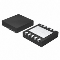
LTC3548EDD-2#TRPBF Linear Technology, LTC3548EDD-2#TRPBF Datasheet

LTC3548EDD-2#TRPBF
Specifications of LTC3548EDD-2#TRPBF
Available stocks
Related parts for LTC3548EDD-2#TRPBF
LTC3548EDD-2#TRPBF Summary of contents
Page 1
... In shutdown, the device draws <1μA. L, LT, LTC, LTM, Linear Technology, the Linear logo and Burst Mode are registered trademarks of Linear Technology Corporation. All other trademarks are the property of their respective owners ...
Page 2
... ORDER INFORMATION LEAD FREE FINISH TAPE AND REEL LTC3548EDD-2#PBF LTC3548EDD-2#TRPBF Consult LTC Marketing for parts specifi ed with wider operating temperature ranges. Consult LTC Marketing for information on non-standard lead based fi nish parts. For more information on lead free part marking, go to: For more information on tape and reel specifi ...
Page 3
ELECTRICAL CHARACTERISTICS temperature range, otherwise specifi cations are at T SYMBOL PARAMETER V Mode Threshold Low MODE Mode Threshold High POR Power-On Reset Threshold Power-On Reset On-Resistance Power-On Reset Delay V RUN Threshold RUN I RUN Leakage Current RUN Note ...
Page 4
LTC3548-2 TYPICAL PERFORMANCE CHARACTERISTICS Effi ciency vs Input Voltage 100 95 100mA 90 10mA 85 1mA 80 800mA 1.8V, CHANNEL 1 OUT 65 Burst Mode OPERATION CIRCUIT OF FIGURE INPUT ...
Page 5
TYPICAL PERFORMANCE CHARACTERISTICS Effi ciency vs Load Current 100 1.5V OUT2 Burst Mode OPERATION 65 NO LOAD ON OTHER CHANNEL ...
Page 6
LTC3548-2 BLOCK DIAGRAM REGULATOR 1 MODE/SYNC 6 + 0.6V EA – OUT1 R1 V FB1 R2 – 0.55V UVDET + + OVDET – 0.65V SHUTDOWN 2 RUN1 0.6V REF OSC 9 RUN2 REGULATOR 2 (IDENTICAL TO REGULATOR 1) ...
Page 7
OPERATION The LTC3548-2 uses a constant-frequency, current mode architecture. The operating frequency is set at 2.25MHz and can be synchronized to an external oscillator. Both channels share the same clock and run in-phase. To suit a variety of applications, the ...
Page 8
LTC3548-2 APPLICATIONS INFORMATION A general LTC3548-2 application circuit is shown in Figure 2. External component selection is driven by the load requirement, and begins with the selection of the inductor L. Once the inductor is chosen, C can be selected. ...
Page 9
APPLICATIONS INFORMATION RMS current must be used. The maximum RMS capacitor current is given by – OUT IN OUT ≈ RMS MAX V IN where the maximum average output current I the peak ...
Page 10
LTC3548-2 APPLICATIONS INFORMATION Great care must be taken when using only ceramic input and output capacitors. When a ceramic capacitor is used at the input and the power is being supplied through long wires, such as from a wall adapter, ...
Page 11
... Hot Swap is a trademark of Linear Technology Corporation. Effi ciency Considerations The percent effi ciency of a switching regulator is equal to the output power divided by the input power times 100%. ...
Page 12
LTC3548-2 APPLICATIONS INFORMATION The R for both the top and bottom MOSFETs can be DS(ON) obtained from the Typical Performance Characteristics 2 curves. Thus, to obtain I R losses losses = OUT ...
Page 13
APPLICATIONS INFORMATION The output voltage can now be programmed by OUT2 choosing the values of R1 and R2. To maintain high effi - ciency, the current in these resistors should be kept small. Choosing 2μA with the 0.6V ...
Page 14
LTC3548-2 PACKAGE DESCRIPTION Low Ripple Buck Regulators Using Ceramic Capacitors V IN 2.5V TO 5.5V C1 RUN2 V IN 10μF LTC3548-2 L2 10μH V OUT2 2.5V SW2 C5 68pF 400mA V FB2 MODE/SYNC 887k 10μF 280k C1, ...
Page 15
... NOTE 6) 0.200 REF Information furnished by Linear Technology Corporation is believed to be accurate and reliable. However, no responsibility is assumed for its use. Linear Technology Corporation makes no representa- tion that the interconnection of its circuits as described herein will not infringe on existing patent rights. DD Package 10-Lead Plastic DFN (3mm × 3mm) (Reference LTC DWG # 05-08-1699 Rev B) 0 ...
Page 16
... V = 0.6V 40μA, IN OUT(MIN 2.5V to 5.5V 0.8V 26μA, IN OUT(MIN 2.5V to 5.5V 0.8V 60μA, IN OUT(MIN 2.5V to 5.5V 0.8V 60μA, IN OUT(MIN 2.25V to 5.5V 0.8V 64μA, IN OUT(MIN 2.5V to 5.5V 0.6V 40μA, IN OUT(MIN 0709 REV B • PRINTED IN USA © LINEAR TECHNOLOGY CORPORATION 2006 35482fb ...


