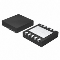
LTC3548EDD#TRPBF Linear Technology, LTC3548EDD#TRPBF Datasheet

LTC3548EDD#TRPBF
Specifications of LTC3548EDD#TRPBF
Available stocks
Related parts for LTC3548EDD#TRPBF
LTC3548EDD#TRPBF Summary of contents
Page 1
... In shutdown, the device draws <1μA. L, LT, LTC, LTM, Linear Technology, the Linear logo and Burst Mode are registered trademarks of Linear Technology Corporation. All other trademarks are the property of their respective owners ...
Page 2
... JA EXPOSED PAD (PIN 11) IS PGND, MUST BE CONNECTED TO GND (SOLDERED TO A 4-LAYER BOARD) ORDER INFORMATION LEAD FREE FINISH TAPE AND REEL LTC3548EDD#PBF LTC3548EDD#TRPBF LTC3548IDD#PBF LTC3548IDD#TRPBF LTC3548EMSE#PBF LTC3548EMSE#TRPBF LTC3548IMSE#PBF LTC3548IMSE#TRPBF Consult LTC Marketing for parts specifi ed with wider operating temperature ranges. *The temperature grade is identifi label on the shipping container. ...
Page 3
ELECTRICAL CHARACTERISTICS temperature range, otherwise specifi cations are at T SYMBOL PARAMETER ΔV Output Voltage Load Regulation LOADREG I Input DC Supply Current S Active Mode Sleep Mode Shutdown f Oscillator Frequency OSC f Synchronization Frequency SYNC I Peak Switch ...
Page 4
LTC3548 TYPICAL PERFORMANCE CHARACTERISTICS Effi ciency vs Input Voltage 100 95 100mA 90 10mA 85 1mA 80 800mA 1.8V, CHANNEL 1 OUT 65 Burst Mode OPERATION CIRCUIT OF FIGURE INPUT ...
Page 5
TYPICAL PERFORMANCE CHARACTERISTICS Effi ciency vs Load Current 100 3.6V 2. 2.5V, CHANNEL 1 OUT 50 Burst Mode OPERATION NO LOAD ON OTHER CHANNEL CIRCUIT OF FIGURE 100 1000 ...
Page 6
LTC3548 BLOCK DIAGRAM REGULATOR 1 MODE/SYNC 6 + 0.6V EA – FB1 – 0.55V UVDET + + OVDET – 0.65V SHUTDOWN RUN1 2 0.6V REF OSC 9 RUN2 REGULATOR 2 (IDENTICAL TO REGULATOR FB2 OPERATION ...
Page 7
OPERATION This decrease causes the error amplifi increase the I voltage until the average inductor current matches the TH new load current. The main control loop is shut down by pulling the RUN pin to ground. Low Current ...
Page 8
LTC3548 APPLICATIONS INFORMATION The inductor value will also have an effect on Burst Mode operation. The transition from low current operation begins when the peak inductor current falls below a level set by the burst clamp. Lower inductor values result ...
Page 9
APPLICATIONS INFORMATION tantalum capacitors are all available in surface mount packages. The OS-CON semiconductor dielectric capacitor available from Sanyo has the lowest ESR (size) product of any aluminum electrolytic at a somewhat higher price. Special polymer capacitors, such as Sanyo ...
Page 10
... Effi ciency = 100% – ( ...) where L1, L2, etc. are the individual losses as a percent- age of input power. Although all dissipative elements in the circuit produce losses, four main sources usually account for most of Hot Swap is a trademark of Linear Technology Corporation. to its steady-state can be monitored OUT , ...
Page 11
APPLICATIONS INFORMATION the losses in LTC3548 circuits switching losses losses, 4) other losses. 1. The V current is the DC supply current given in the IN Electrical Characteristics which excludes MOSFET driver and ...
Page 12
LTC3548 APPLICATIONS INFORMATION Design Example As a design example, consider using the LTC3548 in an portable application with a Li-Ion battery. The battery pro- vides 2.8V to 4.2V. The load requires a maximum IN of 800mA in ...
Page 13
APPLICATIONS INFORMATION V = 2.5V 5.5V C1 10μF RUN2 V RUN1 IN MODE/SYNC POR L2 LTC3548 4.7μ 2.5V* OUT2 SW2 SW1 AT 400mA C5, 68pF V V FB1 FB2 R4 GND C3 R3 887k 4.7μF 280k ...
Page 14
LTC3548 TYPICAL APPLICATIONS 1mm Profi le Core and I/O Supplies 5.5V C1* 10μF RUN2 V IN MODE/SYNC LTC3548 L2 4.7μ 3.3V OUT2 SW2 AT 400mA C5, 68pF V FB2 R4 GND C3 R3 ...
Page 15
... LEAD COPLANARITY (BOTTOM OF LEADS AFTER FORMING) SHALL BE 0.102mm (.004") MAX Information furnished by Linear Technology Corporation is believed to be accurate and reliable. However, no responsibility is assumed for its use. Linear Technology Corporation makes no representa- tion that the interconnection of its circuits as described herein will not infringe on existing patent rights. ...
Page 16
... V = 0.6V 20μA, IN OUT(MIN 2.5V to 5.5V 0.6V 40μA, IN OUT(MIN 2.5V to 5.5V 0.8V 60μA, IN OUT(MIN 2.5V to 5.5V 0.8V 60μA, IN OUT(MIN 2.25V to 5.5V 0.8V 64μA, IN OUT(MIN 2.5V to 5.5V 2.5V 25μA, IN OUT(MIN 0709 REV C • PRINTED IN USA © LINEAR TECHNOLOGY CORPORATION 2005 3548fc ...


