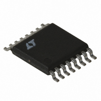
LT1940EFE#TR Linear Technology, LT1940EFE#TR Datasheet

LT1940EFE#TR
Specifications of LT1940EFE#TR
Available stocks
Related parts for LT1940EFE#TR
LT1940EFE#TR Summary of contents
Page 1
... Uses Small Inductors and Ceramic Capacitors Small 16-Lead Thermally Enhanced TSSOP Surface Mount Package U APPLICATIO S Disk Drives DSP Power Supplies Wall Transformer Regulation Distributed Power Regulation DSL Modems Cable Modems , LTC and LT are registered trademarks of Linear Technology Corporation. U TYPICAL APPLICATIO 25V 4.7 F CMDSH-3 BOOST1 0.1 F 3.3 H OUT1 3 ...
Page 2
LT1940/LT1940L ABSOLUTE AXI U RATI GS (Note 1) V Voltage IN LT1940 .................................................... (–0.3), 25V LT1940L ................................................... (–0.3), 7V BOOST Pin Voltage LT1940 ................................................................ 35V LT1940L ............................................................. 16V BOOST Pin Above SW Pin LT1940 ................................................................ 25V LT1940L ...
Page 3
ELECTRICAL CHARACTERISTICS temperature range, otherwise specifications are at T PARAMETER Foldback Frequency Switch Current Limit Switch V CESAT Switch Leakage Current Minimum Boost Voltage Above Switch (Note 4) BOOST Pin Current RUN/SS Current RUN/SS Threshold PG Threshold Offset PG Voltage ...
Page 4
LT1940/LT1940L W U TYPICAL PERFOR A CE CHARACTERISTICS Maximum Load Current 1.8V OUT 1.8 1 2 1.2 1 ...
Page 5
W U TYPICAL PERFOR A CE CHARACTERISTICS RUN/SS Thresholds vs Temperature 1.4 1.2 1.0 TO SWITCH 0.8 0.6 TO RUN 0.4 0.2 0 –50 – 100 125 TEMPERATURE ( C) 1940 G13 ...
Page 6
LT1940/LT1940L W BLOCK DIAGRA 2 A RUN/SS2 2 A RUN/SS1 0.75V SLOPE SLAVE OSC CLK + – 0. RUN/ GND Figure 2. Block Diagram of the LT1940 with Associated External Components ...
Page 7
W BLOCK DIAGRA duty cycle of the power switch, the feedback loop controls the peak current in the switch during each cycle. This current mode control improves loop dynamics and pro- vides cycle-by-cycle current limit. The Block Diagram shows only ...
Page 8
... Also, low inductance may result in discontinuous mode operation, which is okay, but further reduces maximum load current. For details of maximum output current and discontinuous mode operation, see Linear Technology Application Note 44. Finally, for duty cycles greater than 50 ...
Page 9
U U APPLICATIO S I FOR ATIO Table 1. Inductors. Part Number Value I SAT ( H) (A) DC Sumida CR43-1R4 1.4 2.52 CR43-2R2 2.2 1.75 CR43-3R3 3.3 1.44 CR43-4R7 4.7 1.15 CDRH3D16-1R5 1.5 1.55 CDRH3D16-2R2 2.2 1.20 CDRH3D16-3R3 3.3 ...
Page 10
LT1940/LT1940L U U APPLICATIO S I FOR ATIO is likely to see high surge currents when the input source is applied, tantalum capacitors should be surge rated. The manufacturer may also recommend operation below the rated voltage of the capacitor. ...
Page 11
U U APPLICATIO S I FOR ATIO Table 2. Low-ESR Surface Mount Capacitors Vendor Type Taiyo Yuden Ceramic X5R, X7R AVX Ceramic X5R, X7R Tantalum Kemet Tantalum Ta Organic Al Organic Sanyo Organic Panasonic Al Organic TDK ...
Page 12
LT1940/LT1940L U U APPLICATIO S I FOR ATIO The boost circuit can also run directly from a DC voltage that is higher than the input voltage by more than 3V Figure 3d. The diode is used to prevent ...
Page 13
U U APPLICATIO S I FOR ATIO Soft-Start and Shutdown The RUN/SS (Run/Soft-Start) pins are used to place the individual switching regulators and the internal bias cir- cuits in shutdown mode. They also provide a soft-start function. To shut down ...
Page 14
LT1940/LT1940L U U APPLICATIO S I FOR ATIO OFF ON (5a) Channel 2 is Delayed OFF ON OFF2 ON2 (5c) Independent Control of Channel 2 Figure 5. Several Methods of Sequencing the Two Outputs. Channel 1 Starts First. Figure 6. ...
Page 15
U U APPLICATIO S I FOR ATIO GND (7a Figure 7. Subtracting the Current when the Switch is ON (a) From the Current when the Switch is OFF (b) Reveals the Path of the High ...
Page 16
... OUT1 when R4/R3 is small. For example, for 10k 16.5k 10k 243 and R5 = 4.7k. Other Linear Technology Publications Application notes AN19, AN35 and AN44 contain more detailed descriptions and design information for buck regulators and other switching regulators. The LT1376 data sheet has a more extensive discussion of output ripple, loop compensation and stability testing. Design note DN100 shows how to generate a dual (+ and – ...
Page 17
U TYPICAL APPLICATIO S 3.3V and 1.8V Outputs with Sequencing V IN 4.7V TO 14V 4.7 F BOOST1 LT1940 L1 0.1 F 2.2 H OUT1 1.8V SW1 1.4A D1 10.0k FB1 22.6k 20k ...
Page 18
LT1940/LT1940L U TYPICAL APPLICATIO 10V TO 25V C3 D3A 4 3.3 H OUT1 3.3V 1.4A 16.5k C1 15k 10. 330pF 100k PGOOD –5V LOAD SHOULD BE LESS THAN 1/2 5V LOAD (SEE DESIGN ...
Page 19
... DRAWING NOT TO SCALE Information furnished by Linear Technology Corporation is believed to be accurate and reliable. However, no responsibility is assumed for its use. Linear Technology Corporation makes no represen- tation that the interconnection of its circuits as described herein will not infringe on existing patent rights. TFT LCD Supply D4B 4 ...
Page 20
... A OUT(MIN 34V <1 A, OUT(MAX 34V <1 A, OUT(MAX 34V <1 A, OUT(MAX 1.2V 2.5mA OUT(MIN 0.6V MSE Package OUT(MIN 0.8V <1 A OUT(MIN 0.8V <1 A OUT(MIN 1.20V 2.5mA OUT(MIN 0.8V 460 OUT(MIN LT/TP 0204 1K REV A • PRINTED IN USA LINEAR TECHNOLOGY CORPORATION 2001 1940fa ...


