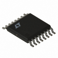
LT1940EFE#TR Linear Technology, LT1940EFE#TR Datasheet - Page 6

LT1940EFE#TR
Manufacturer Part Number
LT1940EFE#TR
Description
IC REG SW DUAL 1.4A STDN 16TSSOP
Manufacturer
Linear Technology
Type
Step-Down (Buck)r
Datasheet
1.LT1940EFEPBF.pdf
(20 pages)
Specifications of LT1940EFE#TR
Internal Switch(s)
Yes
Synchronous Rectifier
No
Number Of Outputs
2
Voltage - Output
1.25 ~ 22 V
Current - Output
1.4A
Frequency - Switching
1.1MHz
Voltage - Input
3.6 ~ 25 V
Operating Temperature
-40°C ~ 85°C
Mounting Type
Surface Mount
Package / Case
16-TSSOP Exposed Pad, 16-eTSSOP, 16-HTSSOP
Lead Free Status / RoHS Status
Contains lead / RoHS non-compliant
Power - Output
-
Available stocks
Company
Part Number
Manufacturer
Quantity
Price
BLOCK DIAGRA
LT1940/LT1940L
The LT1940 is a dual, constant frequency, current mode
buck regulator with internal 2A power switches. The two
regulators share common circuitry including input source,
voltage reference and oscillator, but are otherwise inde-
pendent. This section describes the operation of the
LT1940; refer to the Block Diagram.
If the RUN/SS (run/soft-start) pins are both tied to ground,
the LT1940 is shut down and draws 30 A from the input
source tied to V
external soft-start capacitors, generating voltage ramps at
6
C
F
CLK
Figure 2. Block Diagram of the LT1940 with Associated External Components (One of Two Switching Regulators Shown)
RUN/SS2
RUN/SS1
R
C
C
GND
V
C
PG
C
RUN/SS
2 A
2 A
SLOPE
IN
+
–
. Internal 2 A current sources charge
SLAVE
OSC
0.5V
W
0.75V
AND REF
INT REG
C1
V
IN
–
+
CLAMP
I
LIMIT
R
S
MASTER
OSC
Q
CLK1
CLK2
ERROR
these pins. If either RUN/SS pin exceeds 0.6V, the internal
bias circuits turn on, including the internal regulator,
1.25V reference and 1.1MHz master oscillator. In this
state, the LT1940 draws 3.5mA from V
both RUN/SS pins are high. Neither switching regulator
will begin to operate until its RUN/SS pin reaches ~0.8V.
The master oscillator generates two clock signals of
opposite phase.
The two switchers are current mode step-down regula-
tors. This means that instead of directly modulating the
AMP
–
+
+
–
125mV
1.25V
1940 F02
BOOST
SW
V
FB
IN
R2
C
D1
IN
IN
C3
D2
L1
R1
IN
, whether one or
C1
OUT
1940fa


