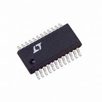
LTC3736EGN-1 Linear Technology, LTC3736EGN-1 Datasheet - Page 7

LTC3736EGN-1
Manufacturer Part Number
LTC3736EGN-1
Description
IC CTRLR SW SYNC DUAL 2PH 24SSOP
Manufacturer
Linear Technology
Series
PolyPhase®r
Type
Step-Down (Buck)r
Datasheet
1.LTC3736EGN-1.pdf
(28 pages)
Specifications of LTC3736EGN-1
Internal Switch(s)
No
Synchronous Rectifier
Yes
Number Of Outputs
2
Voltage - Output
0.6 ~ 9.8 V
Current - Output
1A
Frequency - Switching
450kHz ~ 580kHz
Voltage - Input
2.75 ~ 9.8 V
Operating Temperature
-40°C ~ 85°C
Mounting Type
Surface Mount
Package / Case
24-SSOP
Lead Free Status / RoHS Status
Contains lead / RoHS non-compliant
Power - Output
-
PI FU CTIO S
TG1/TG2 (Pins 17, 15/Pins 20, 18): Top (PMOS) Gate Drive
Output. These pins drive the gates of the external P-channel
MOSFETs. These pins have an output swing from PGND to
SENSE
SSDIS (Pin 18/Pin 21): Spread Spectrum Disable Input. Tie
this pin to V
mode, the LTC3736-1 operates at a constant frequency
determined by the voltage on the FREQ pin. Tie this pin to
GND to enable spread spectrum operation.
BG1/BG2 (Pins 19, 13/Pins 22, 16): Bottom (NMOS) Gate
Drive Output. These pins drive the gates of the external N-
channel MOSFETs. These pins have an output swing from
PGND to SENSE
SENSE1
Input to Differential Current Comparator. Also powers the
gate drivers. Normally connected to the source of the ex-
ternal P-channel MOSFET.
FU CTIO AL DIAGRA
U
U
+
.
+
/SENSE2
U
IN
to disable spread spectrum operation. In this
U
+
.
+
U
(Pins 21, 11/Pins 24, 14): Positive
RUN/SS
SSDIS
FREQ
IPRG1
IPRG2
UNDERVOLTAGE
LOCKOUT
(UF/GN Package)
0.7µA
SENSE VOLTAGE
CONTROLLED
OSCILLATOR
OSCILLATOR
SPECTRUM
MAXIMUM
VOLTAGE
SPREAD
SELECT
W
V
IN
EXTSS
REFERENCE
VOLTAGE
(Common Circuitry)
CLK1
CLK2
SHDN
t
SEC
IPROG1
IPROG2
C
VIN
= 1ms
R
0.6V
V
VIN
REF
V
(TO CONTROLLER 1, 2)
0.54V
IN
SLOPE
COMP
V
V
+
–
FB1
FB2
SW1/SW2 (Pins 22, 10/Pins 1, 13): Switch Node Connec-
tion to Inductor. Also the negative input to differential peak
current comparator and an input to the reverse current
comparator. Normally connected to the drain of the exter-
nal P-channel MOSFETs, the drain of the external N-channel
MOSFET and the inductor.
IPRG1/IPRG2 (Pins 23, 2/Pins 2, 5): Three-State Pins to
Select Maximum Peak Sense Voltage Threshold. These pins
select the maximum allowed voltage drop between the
SENSE
across the external P-channel MOSFET) for each channel.
Tie to V
respectively.
V
the remotely sensed feedback voltage for its controller from
an external resistor divider across the output.
Exposed Pad (Pin 25/NA): The exposed pad (UF Package)
must be soldered to the PCB ground.
FB1
–
+
+
–
/V
FB2
+
IN
SLOPE1
SLOPE2
and SW pins (i.e., the maximum allowed drop
, GND or float to select 204mV, 85mV or 125mV
(Pins 24, 7/Pins 3, 10): Feedback Pins. Receives
INTSS
UV1
UV2
OV1
SHDN
OV2
PGOOD
37361 FD
LTC3736-1
37361f
7


